

Electrical assembly with internal memory circuitized substrate having electronic components positioned thereon, method of making same, and information handling system utilizing same
a technology of circuitized substrates and electrical assemblies, applied in the field of circuitized substrates, can solve the problems of significant signal transmission concerns, increased complexity of pcb and other substrates, and increased complexity of signal behavior
- Summary
- Abstract
- Description
- Claims
- Application Information
AI Technical Summary
Benefits of technology
Problems solved by technology
Method used
Image

Examples
Embodiment Construction
[0038] For a better understanding of the present invention, together with other and further objects, advantages and capabilities thereof, reference is made to the following disclosure and appended claims in connection with the above-described drawings. It is understood that like numerals will be used to indicate like elements from FIG. to FIG.
[0039] The following terms will be used herein and are understood to have the meanings associated therewith.
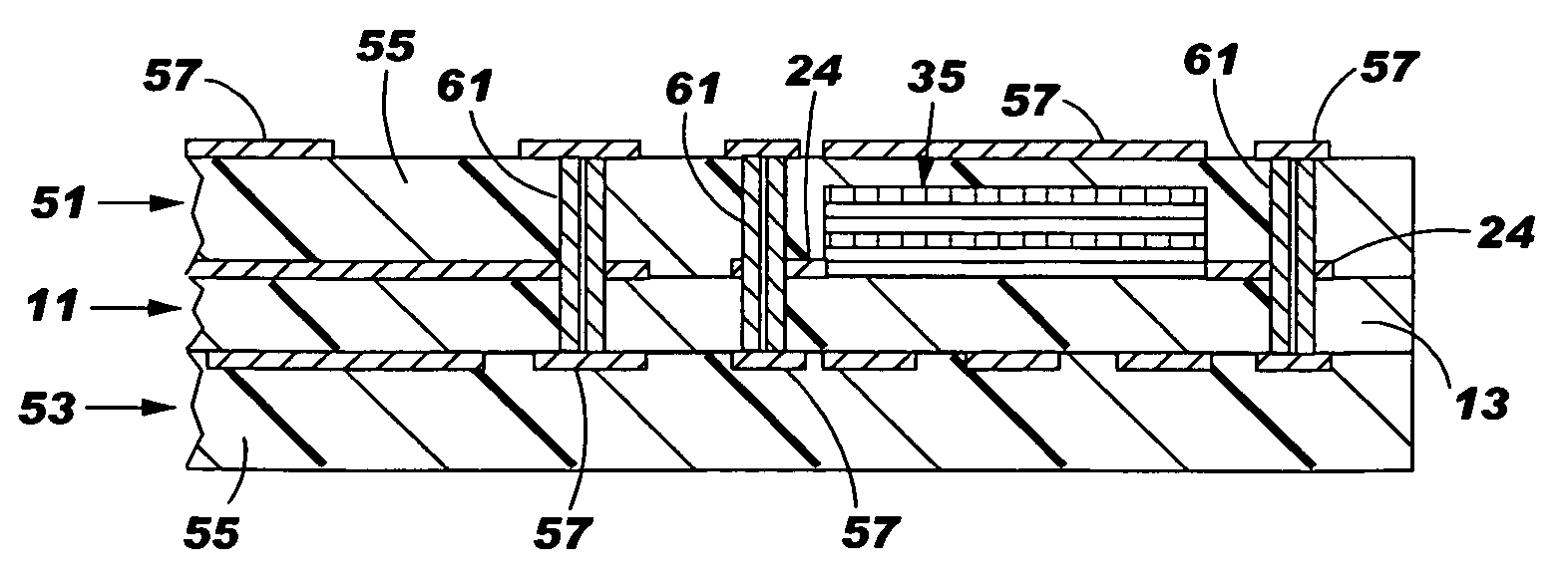
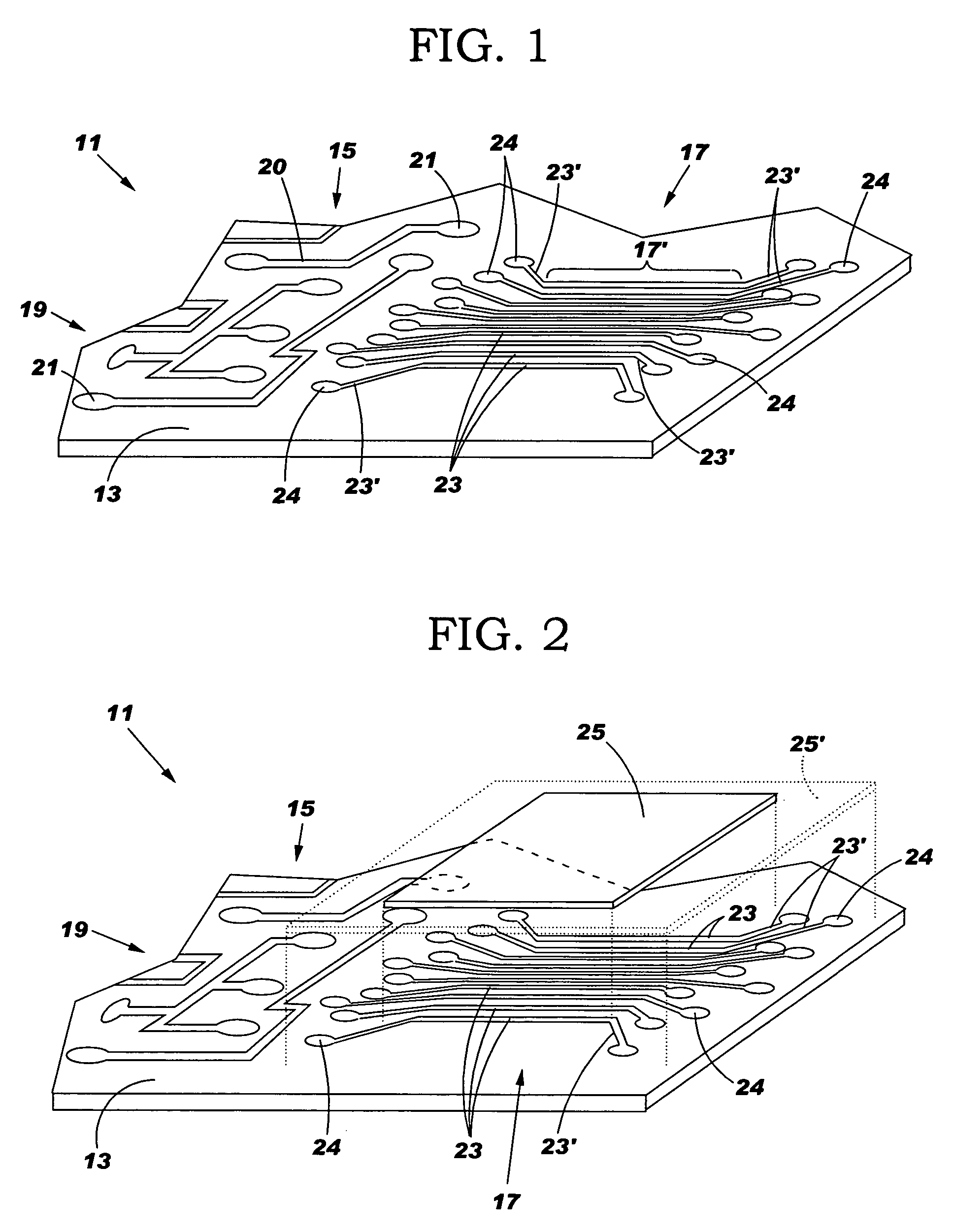
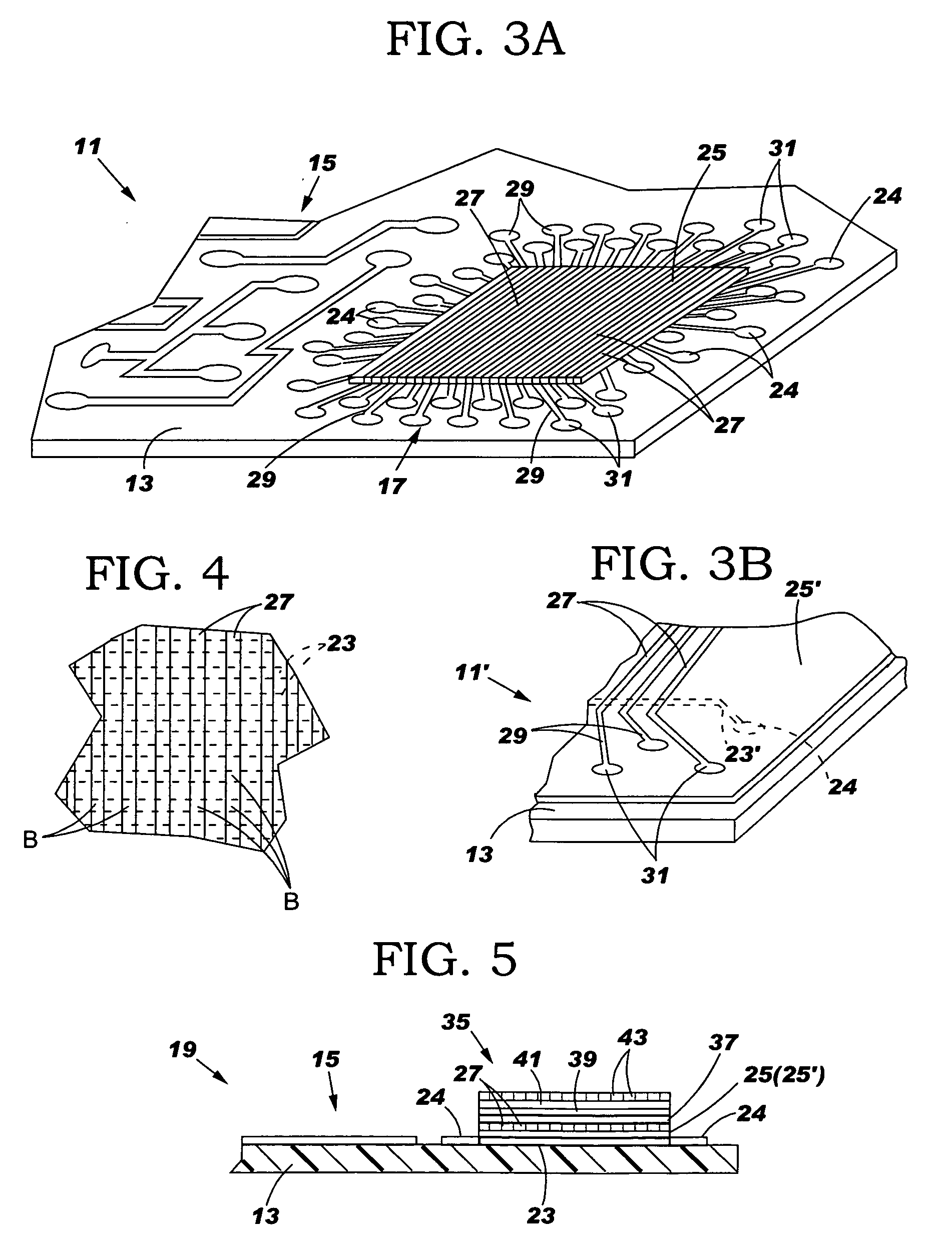
[0040] By the term “circuitized substrate” is meant to include substrates having at least one dielectric layer and one conductive layer. In many cases, such substrates will include several dielectric and conductive layers. Examples include printed circuit boards (PCBs) or like structures made of dielectric materials such as fiberglass-reinforced epoxy resins, polytetrafluoroethylene (Teflon), polyimides, polyamides, cyanate resins, photoimageable materials, and other like materials wherein the conductive layer is a metal layer (e.g., po...
PUM
 Abstract
Description
Claims
Application Information