Semiconductor device and method for manufacturing the same

a semiconductor device and structure technology, applied in the direction of recording information storage, maintaining head carrier alignment, instruments, etc., can solve the problems of increasing the cost of manufacturing semiconductor devices, affecting the quality of semiconductor devices, so as to achieve excellent chemical resistance and fine processing

Inactive Publication Date: 2006-02-02
CANON KK
View PDF6 Cites 11 Cited by
  • Summary
  • Abstract
  • Description
  • Claims
  • Application Information

AI Technical Summary

Benefits of technology

[0010] Therefore, an object of the present invention is to provide a semiconductor device having interlayer insulating layers that excel...

Problems solved by technology

With the miniaturization of semiconductor devices in recent years, wiring capacity has increased, and the delay of signals through wirings has become significant.
However, since the film quality of porous bodies composed of organic materials or the mixture of organic and inorganic materials is significantly different from the film quality of a silicon oxide film or the like used as the material of interlayer insulating films in conventional semiconductor devices, various new processes are required leading to the rise of costs for manufacturing the semiconductor devices.
In addition, there are many ma...

Method used


Image

  • Semiconductor device and method for manufacturing the same
  • Semiconductor device and method for manufacturing the same
  • Semiconductor device and method for manufacturing the same

Examples


first example

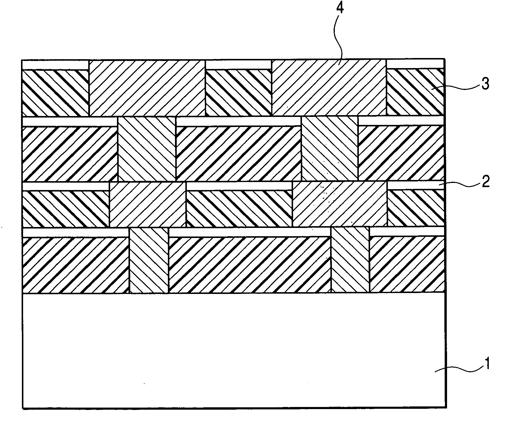
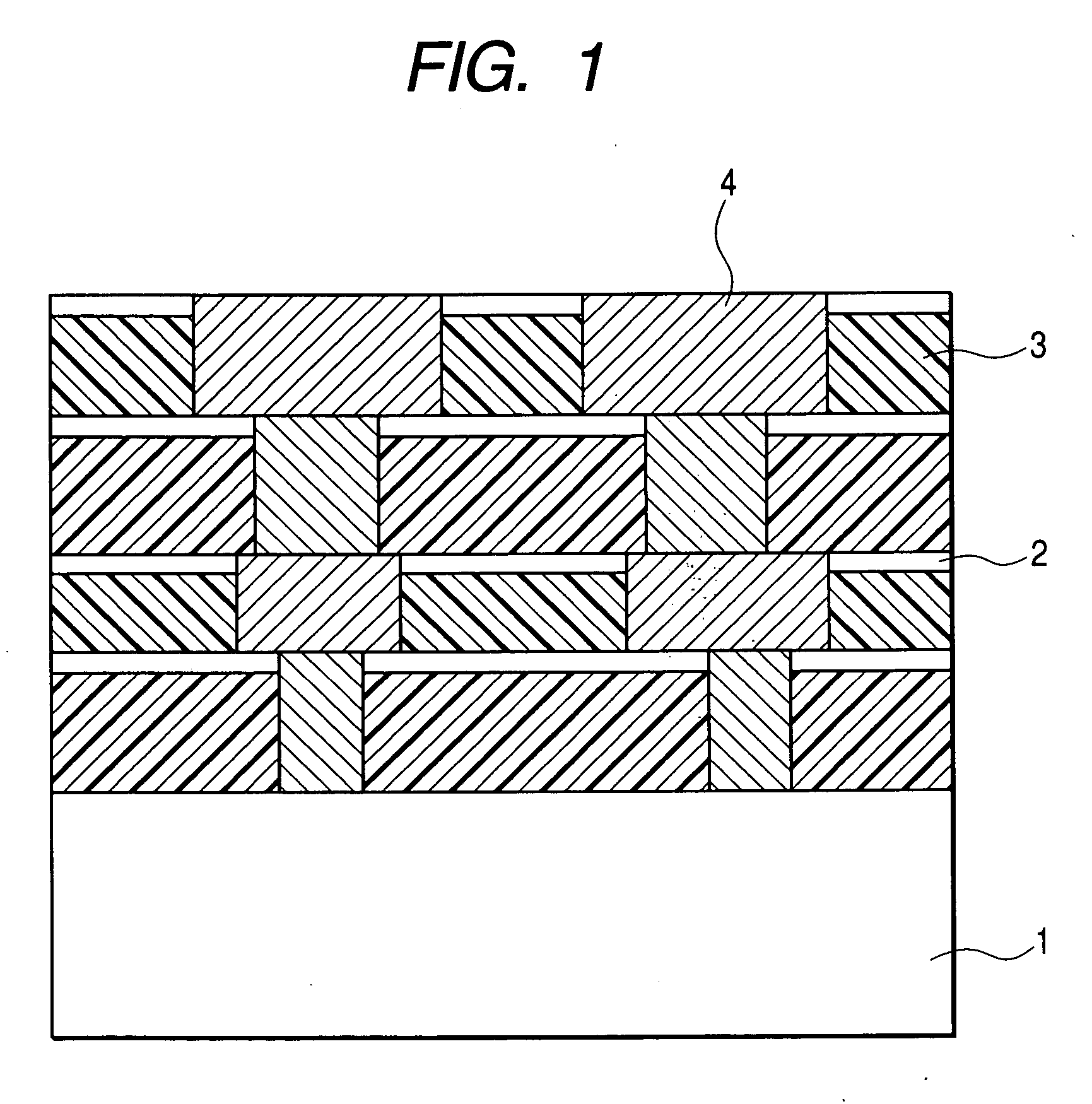
[0082] The first example is an example of a semiconductor device wherein porous films having fine pores perpendicular to a substrate consisting mainly of silicon oxide are used as interlayer insulating layers, and wirings are formed by burying aluminum in the fine pores in the porous film. Here, an example of forming a via, which is a vertical wiring, is formed in the interlayer insulating layers will be described.

[0083] As described above, FIGS. 3A to 3D schematically show the manufacturing steps for forming interlayer insulating layers and metal wirings thereon. The manufacturing method will be described below referring to FIGS. 3A to 3D.

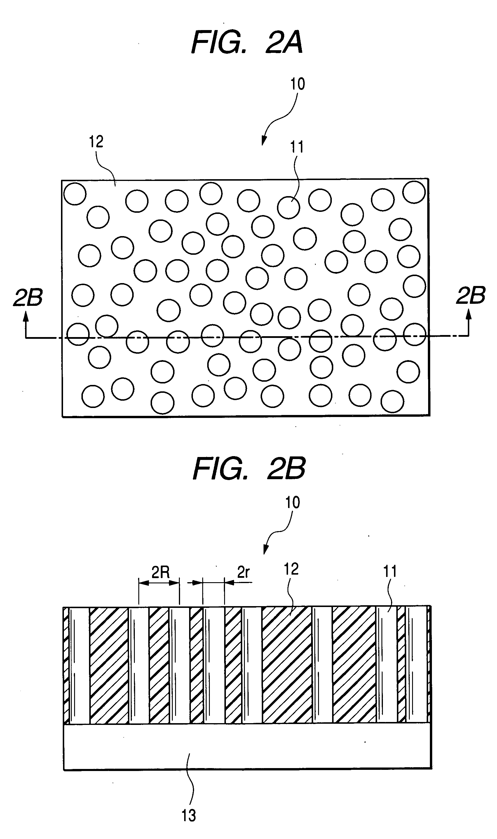
[0084] First, on a semiconductor substrate on which semiconductor elements such as MOSFET, wiring layers and element isolating regions (not shown) were formed, an aluminum-silicon mixture (mixed film) 20 containing 60 atomic % aluminum relative to the total quantity of aluminum and silicon as shown in FIG. 3A was formed using a magnetron sputter...

second example

[0094] The second example is an example of a semiconductor device wherein porous films having fine pores perpendicular to a substrate consisting mainly of silicon oxide are used as interlayer insulating layers, and metal wirings (via) are formed by burying Cu in the fine pores. Here, an example of forming a via, which is a vertical wiring, is formed in the interlayer insulating layers will be described.

[0095] As described above, FIGS. 4A to 4F schematically show the manufacturing steps for forming interlayer insulating layers and metal wirings thereon. The manufacturing method will be described below referring to FIGS. 4A to 4F.

[0096] First, on a semiconductor substrate 31 on which semiconductor elements such as MOSFET, wiring layers and element isolating regions (not shown) were formed, an aluminum-silicon mixture (mixed film) 30 containing 60 atomic % aluminum to the total quantity of aluminum and silicon as shown in FIG. 4A was formed using a magnetron sputtering method. As the...

third example

[0107] The third example is an example of a semiconductor device wherein porous films having fine pores perpendicular to a substrate consisting mainly of silicon oxide are used as interlayer insulating layers, and Cu was buried in the region after removing a part of the porous films as metal wirings.

[0108] As described above, FIGS. 5A to 5F schematically show the manufacturing steps for forming interlayer insulating layers and metal wirings thereon. The manufacturing method will be described below referring to FIGS. 5A to 5F.

[0109] First, on a semiconductor substrate on which semiconductor elements such as MOSFET, wiring layers and element isolating regions (not shown) were formed, an aluminum-silicon mixture (mixed film) 40 containing 60 atomic % aluminum to the total quantity of aluminum and silicon as shown in FIG. 5A was formed using a magnetron sputtering method. As the target, a circular aluminum-silicon mixed target of a diameter of 4 inches (101.6 mm) fabricated by mixing ...


PUM


Abstract

A semiconductor device has multi-layered interlayer insulating layers 3 formed on a semiconductor substrate 1, and wirings 4 formed in the interlayer insulating layers 3. The interlayer insulating layers 3 are composed of porous bodies having fine columnar pores and parent-material regions consisting mainly of silicon oxides surrounding the fine pores. The wirings 4 are composed of structures wherein columnar substances containing aluminum are dispersed in a base material containing silicon, or regions wherein an electrically conductive material is introduced in a portion of the porous bodies. The average diameter of the fine pores in the porous bodies is 1 nm or larger and 10 nm or smaller, and the average distance between the fine pores is 3 nm or larger and 15 nm or smaller. The fine pores in the porous bodies is formed perpendicularly, or substantially perpendicularly to the film surface on a semiconductor substrate 1.

Description

[0001] This is a continuation-in-part application of U.S. patent application Ser. No. 10 / 271,472 filed on Oct. 15, 2002.BACKGROUND OF THE INVENTION [0002] 1. Field of the Invention [0003] The present invention relates to a semiconductor device having a novel structure and a method for manufacturing the same; and more specifically to a semiconductor device having multi-layer wirings of a lowered wiring capacity by the use of a low-dielectric-constant film of a novel structure, and a method for manufacturing the same. [0004] 2. Related Background Art [0005] With the miniaturization of semiconductor devices in recent years, wiring capacity has increased, and the delay of signals through wirings has become significant. For lowering wiring capacity, the reduction of the resistance of metal wiring, and the use of materials having a low specific dielectric constant as interlayer insulating films can be considered. In general, as a method for reducing the resistance of metal wiring, the cha...

Claims


Application Information

Patent Timeline
IPC IPC(8): H01L23/52G11B5/596G11B5/73G11B5/74G11B5/82G11B5/855
CPCG11B5/59633G11B5/7325H01L2924/0002G11B5/74G11B5/82G11B5/855H01L21/7682H01L21/76838H01L21/76877H01L21/76879H01L21/76888H01L23/5222H01L23/53295H01L2221/1094H01L2924/00G11B5/743H01L23/52
Inventor FUKUTANI, KAZUHIKODEN, TOHRUMIYATA, HIROKATSU
Owner CANON KK
Why Eureka
Try Eureka