

Silver plating in electronics manufacture
- Summary
- Abstract
- Description
- Claims
- Application Information
AI Technical Summary
Benefits of technology
Problems solved by technology
Method used
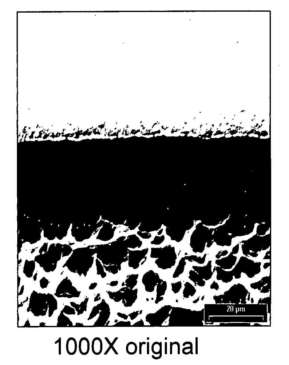
Image

Examples
example 1
[0086] Laminated Cu panels (3 cm×5 cm) were prepared by cleaning, etching, and pre-dip per manufacturers' recommended procedures. Panels were plated in accordance with a process of the invention, employing a plating composition with the following components:
AgNO30.79g / LHEDTA10g / Lbenzimidazole1g / L3,5 dinitrohydroxy0g / Lbenzoic acidnon-ionic surfactant1g / LEO / PO block co-polymerpolyethyleneglycol0g / LHNO30.98g / LD.I. waterbalance
The operating pH began at about 2.
[0087] Additional panels were plated with Ag by a process not of the invention employing a commercially available plating composition. The operating pH began at less than 1.
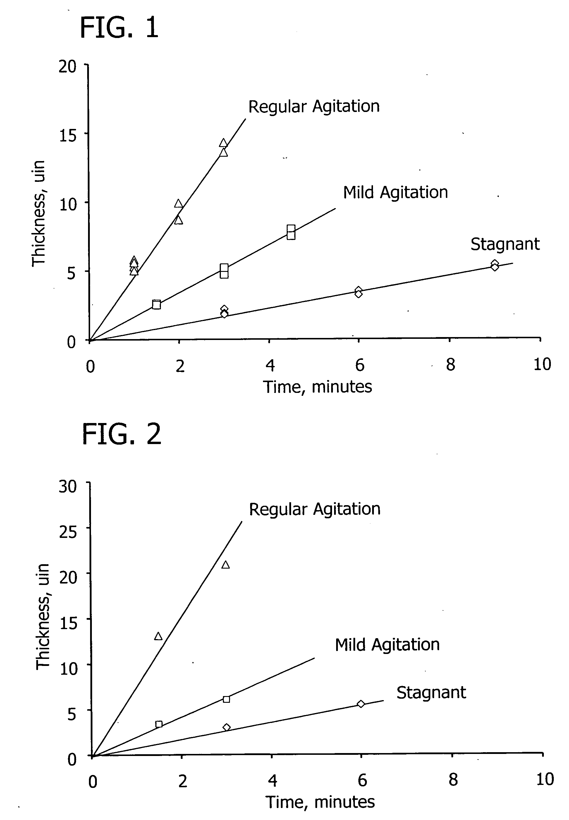
[0088] To encompass the various hydrodynamic conditions from production lines, plating was conducted at three agitation conditions: stagnant, mild agitation, and regular agitation (estimated linear speeds of 0, 1.6, and 3.2 cm / s, respectively). Samples were plated for different lengths of time to generate a wide range of silver thickness. Panels of laminat...
example 2
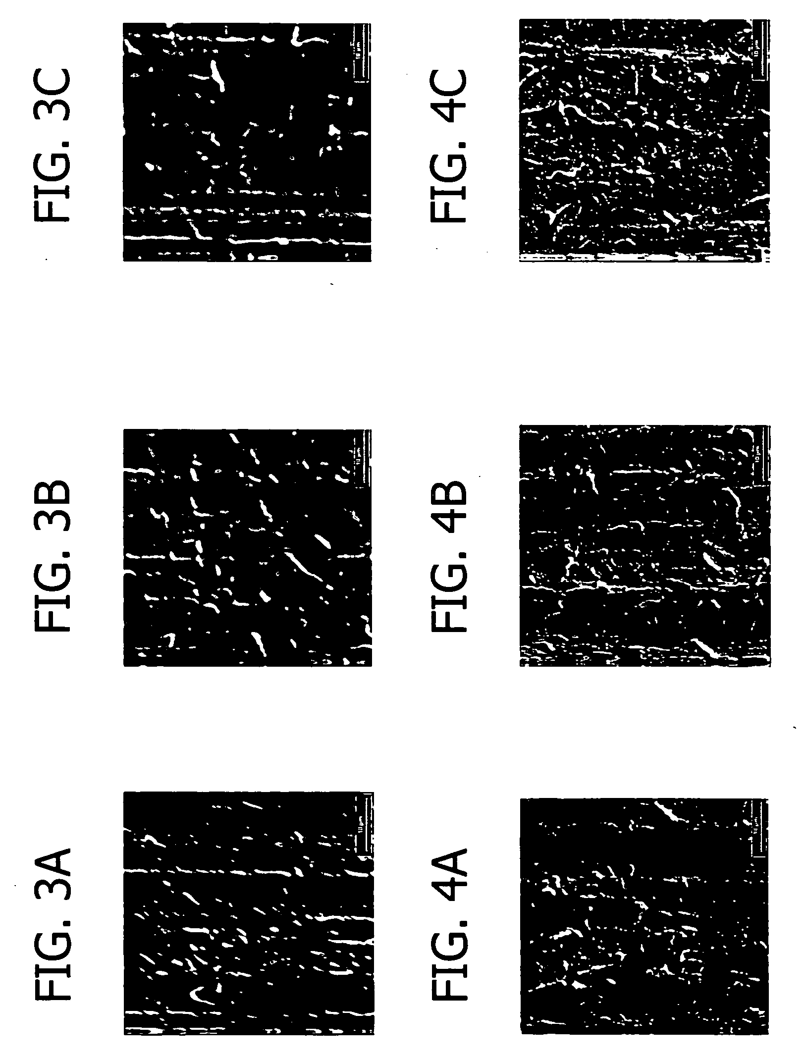
[0090] The panels of Example 1 were examined under scanning electron microscope (SEM) and photomicrographs were taken. FIG. 3 (3A, 3B, 3C) shows Ag coatings not of the invention taken at 2000× magnification of panels representing the following three data points of FIG. 1:
[0091]FIG. 3A: 3 μin thick; 3 mins.; stagnant
[0092]FIG. 3B: 13 μin thick; 1.5 mins.; agitation
[0093]FIG. 3C: 21 μin thick; 2 mins.; agitation
[0094]FIG. 4 (4A, 4B, 4C) shows Ag coatings of the invention taken at 2000× magnification of panels representing the following three data points of FIG. 2:
[0095]FIG. 4A: 4 μin thick; 6 mins.; stagnant
[0096]FIG. 4B: 6 μin thick; 2 mins.; mild agitation
[0097]FIG. 4C: 8 μin thick; 2 mins.; agitation
[0098] These figures show that the coating morphology remains unchanged as the thickness increases and conditions otherwise change for both processes. The Ag from the process of the invention (FIG. 4) appears to have a finer grain structure, which was confirmed by X-ray diffract...
example 3
[0099] Tarnish resistance was evaluated by visual inspection after exposure to conditions of 85 C and 85% RH (relative humidity) for 24 hours. FIG. 5 shows Ag coatings of the invention on test panels representing the following process conditions:
[0100]FIG. 5A: 4 μin thick; 6 mins.; stagnant
[0101]FIG. 5B: 5 μin thick; 2 mins.; mild agitation
[0102]FIG. 5C: 12 μin thick; 3 mins.; agitation
[0103]FIG. 6 shows Ag coatings not of the invention representing the following conditions:
[0104]FIG. 6A: 3 μin thick; 3 mins.; stagnant
[0105]FIG. 6B: 6 μin thick; 3 mins.; mild agitation
[0106]FIG. 6C: 21 μin thick; 3 mins.; agitation
[0107] These photos show that the Ag coating is heavily tarnished at thicknesses of 3 and 6 μin applied by the comparative process, while the Ag coating is only slightly tarnished for all thicknesses 4, 5, and 12 μin applied by the process of the invention.
PUM
| Property | Measurement | Unit |
|---|---|---|
| Fraction | aaaaa | aaaaa |
| Electrical conductivity | aaaaa | aaaaa |
| Electrical conductivity | aaaaa | aaaaa |
Abstract
Description
Claims
Application Information