Methods to provide and expose a diagnostic connector on overmolded electronic packages

a technology of electronic components and connectors, which is applied in the direction of resistive material coating, metallic pattern materials, and test/measurement of semiconductor/solid-state devices, etc., can solve the problems of difficult to determine the faulty area of the electronic circuit or the failure of the electronic device, so as to facilitate failure analysis and instrumentation, and reduce the risk of damage to the circuit and electronic device. , the effect of reducing the risk of damag

Active Publication Date: 2006-02-09
DELPHI TECH IP LTD
View PDF26 Cites 4 Cited by
  • Summary
  • Abstract
  • Description
  • Claims
  • Application Information

AI Technical Summary

Benefits of technology

[0011] Advantageously, the present invention facilitates failure analysis and instrumentation used during product development of an encapsulated electronic assembly with minimal decapsulation of the overmolding material and with substantially reduced risk of damaging the circuit and electronic devices. The present invention further provides an inexpensive and efficient method of sealing an electronic assembly from environmentals while facilitating simplified and efficient diagnostic connection for failure analysis.

Problems solved by technology

Although the above-described assembly process provides a package, which may be disassembled for failure analysis of the electronic devices, the assembly process is labor intensive and involves a number of components.
However, the overmolding or sealing material presents a difficult obstacle for subsequent failure analysis.
Because the entire electronic assembly or at least all electronic devices is generally encapsulated with the overmolding material, it is difficult to determine the faulty area of the electronic circuit or which electronic device is malfunctioning or failed.
Decapsulation of the entire circuit board and electronic devices is very difficult and time consuming and may lead to damage of the electronic devices or circuit board.

Method used


Image

  • Methods to provide and expose a diagnostic connector on overmolded electronic packages
  • Methods to provide and expose a diagnostic connector on overmolded electronic packages
  • Methods to provide and expose a diagnostic connector on overmolded electronic packages

Examples


Embodiment Construction

[0029] The embodiments disclosed below are not intended to be exhaustive or limit the invention to the precise forms disclosed in the following detailed description. Rather, the embodiments are chosen and described so that others skilled in the art may utilize their teachings.

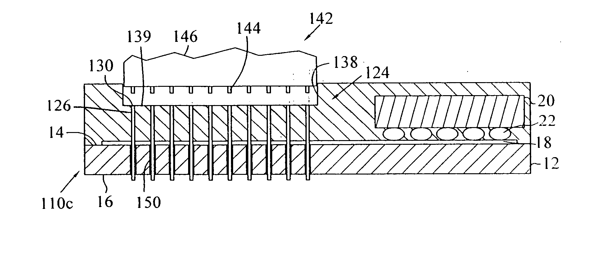
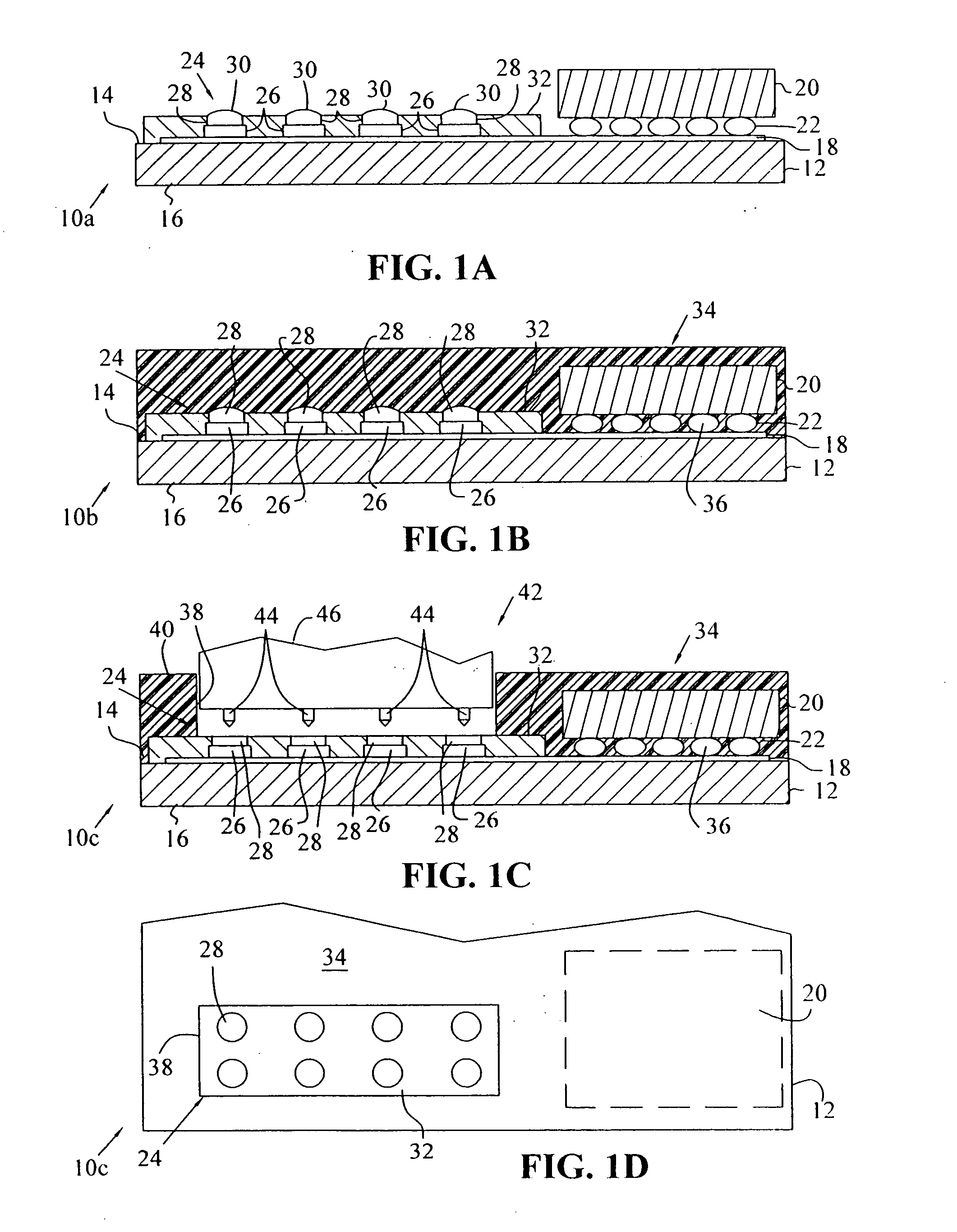
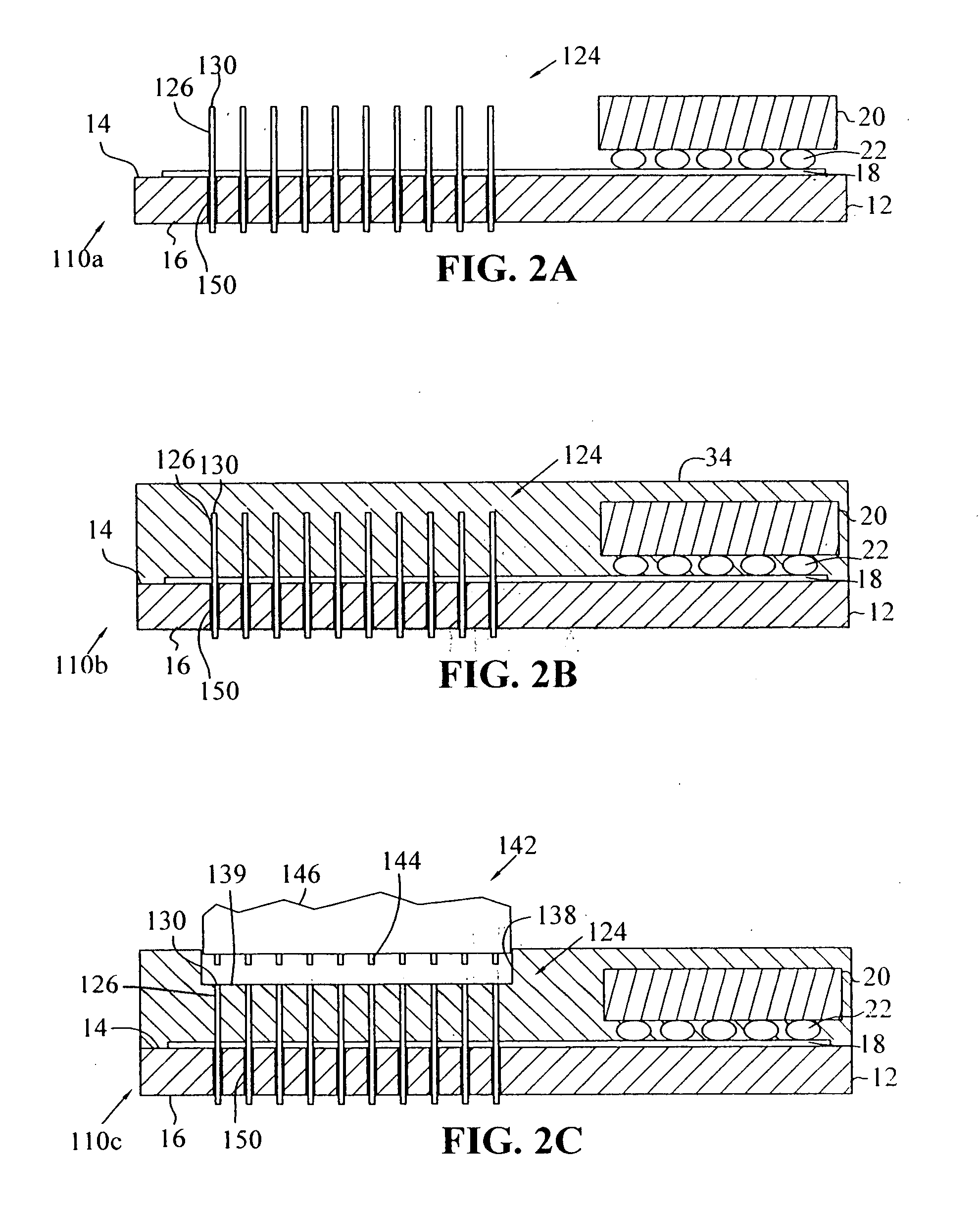
[0030]FIGS. 1A-1D represent a first exemplary embodiment and method of providing and exposing a diagnostic connection for an overmolded electronic assembly. Referring to FIG. 1A, electronic assembly 10a includes circuit board 12 having a first side surface 14 and an oppositely located second side surface 16. Circuit board 12 may be a laminate, printed circuit board (PCB), ceramic, or any other suitable substrate or other circuit board material known in the art. Circuit board 12 may include electrical circuit 18 printed, for example, on first side 14; however, circuit 18 may be provided and located in an alternative form or location. Additionally, electronic assembly 10a includes components such as electronic d...


PUM

PropertyMeasurementUnit
heightaaaaaaaaaa
pressureaaaaaaaaaa
electricalaaaaaaaaaa

Abstract

An overmolded electronic assembly is provided having a circuit board with electronic devices and a diagnostic connection. The diagnostic connection includes electrical conductors having a distal end projecting above a first side of the circuit board, for example, circuit pads having solder thereon or conductive pins oriented substantially perpendicular to the circuit board. The electrical conductors are overmolded with sealing material along with the other electronic devices and circuit board area. The sealing material is a dielectric, for example, a thermoset polymer base such as epoxy that may include another material such as a fill material. In order to provide a diagnostic connection to the circuit and electronic devices, the encapsulation or sealing material overlying the electrical conductors is removed from the outside surface down to at least the distal end of the electrical conductors. The arrangement of the electrical conductors and the method of removal of the sealing material prevents damage to the circuit and electronic devices and provides instrumentation used during product development and facilitates failure analysis. The sealing material may be removed, for example, by mechanical cutting, laser cutting, or high pressure jet erosion, for example, by a high pressure water or liquid nitrogen stream.

Description

TECHNICAL BACKGROUND [0001] The present invention relates to diagnostic connections for overmolded electronic assemblies that include a circuit board having electronic devices. BACKGROUND OF THE INVENTION [0002] Circuit boards with electronic devices, for example, flip chips or other semiconductors, must often be protected from the environment in which the board is employed. The method of protection generally must also allow a method of accessing the electronic devices for failure analysis. [0003] One widely practiced protection approach is to enclose a circuit board in an assembly composed of a pair of case halves. The case halves are secured together with fasteners to form an enclosure that supports and protects the circuit board and electronic devices within. The assembly typically includes a sealing material between the case halves to exclude moisture from the enclosure. The resulting package must then be tested for leakage to ensure the package was properly assembled and sealed...

Claims


Application Information

Patent Timeline
Patent Type & Authority Applications(United States)
IPC IPC(8): H05K1/03H05K3/00
CPCG01R3/00H05K1/0268H05K2201/10303H05K3/288H05K3/284H01L2924/181H01L2224/16225H01L2924/00012
Inventor BRANDENBURG, SCOTT D.TSAI, JEENHUEI S.
Owner DELPHI TECH IP LTD
Why Eureka
Try Eureka