Method of forming strained silicon materials with improved thermal conductivity

a technology of strained silicon and thermal conductivity, which is applied in the direction of basic electric elements, semiconductor devices, electrical equipment, etc., can solve the problems of poor thermal conductivity of sige alloy materials, degrade the dc characteristics of transistors fabricated on the bilayer structure, and device fabrication in a si/sige bilayer structur

Active Publication Date: 2006-02-09
GLOBALFOUNDRIES US INC
View PDF5 Cites 9 Cited by
  • Summary
  • Abstract
  • Description
  • Claims
  • Application Information

AI Technical Summary

Problems solved by technology

Regardless of how the substrates are made, a substantial obstacle to device fabrication in a Si/SiGe bilayer structure is the poor thermal conductivity of the SiGe alloy material.
This has been shown to degrade the DC characteristics of transistors fabricated on the bilayer structure.
Since heat cannot be transported away as quickly as in the case of pure Si, the temperature in the channel region of the

Method used


Image

  • Method of forming strained silicon materials with improved thermal conductivity
  • Method of forming strained silicon materials with improved thermal conductivity
  • Method of forming strained silicon materials with improved thermal conductivity

Examples


Embodiment Construction

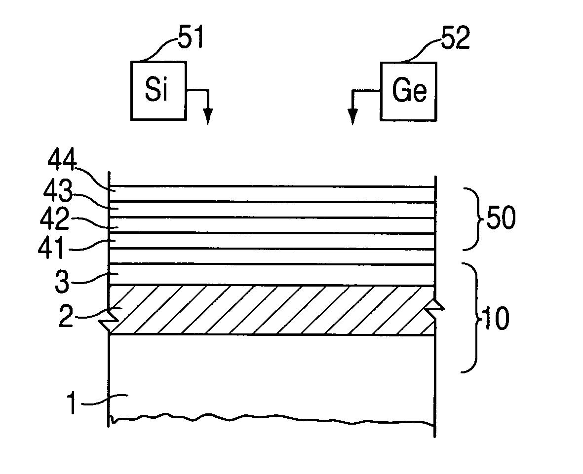
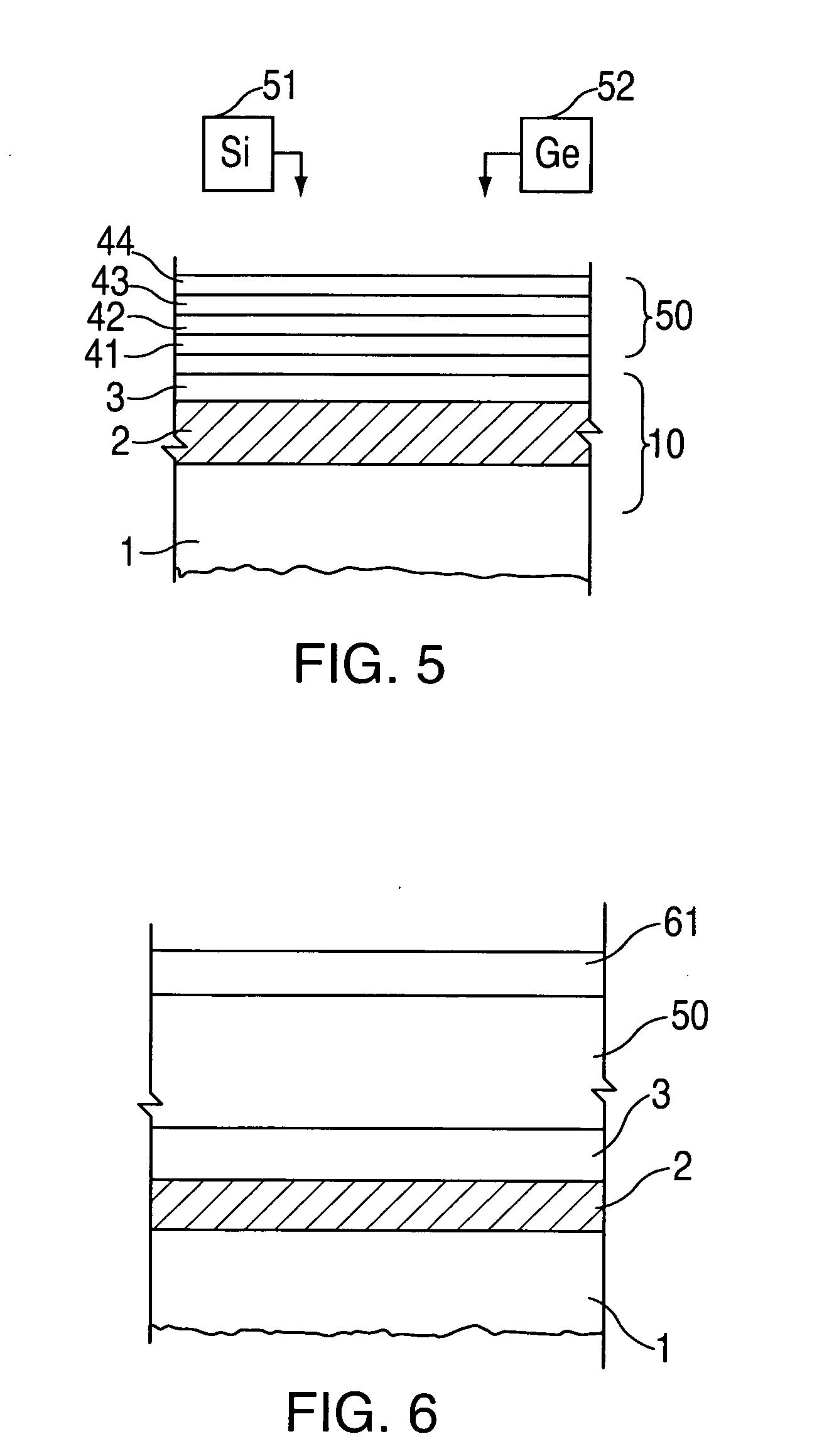
[0018] In accordance with the present invention, a layer of SiGe alloy is formed on a substrate (typically bulk Si, SOI or SGOI); the SiGe alloy layer has reduced mass variance and hence higher thermal conductivity than a layer of random SiGe alloy. This is accomplished by forming the SiGe layer as an ordered digital alloy, as opposed to a random alloy.

[0019]FIG. 5 illustrates a SiGe digital alloy formed by the process of the present invention. The substrate 10 (here shown as an SOI structure with Si layer 3 and insulator 2 on bulk substrate 1) is placed in a processing chamber where layers of either Si or Ge may be deposited on the substrate using Si and Ge sources 51, 52. A variety of deposition techniques may be used, including ultrahigh-vacuum CVD (UHVCVD) and low-temperature epitaxy (LTE), preferably at temperatures less than 650° C.

[0020] A thin layer 41 of Si is deposited on the substrate, and a thin layer 42 of Ge is deposited on layer 42. Alternating layers 43, 44, etc. o...


PUM


Abstract

A method is disclosed for forming a strained Si layer on SiGe, where the SiGe layer has improved thermal conductivity. A first layer of Si or Ge is deposited on a substrate in a first depositing step; a second layer of the other element is deposited on the first layer in a second depositing step; and the first and second depositing steps are repeated so as to form a combined SiGe layer having a plurality of Si layers and a plurality of Ge layers. The respective thicknesses of the Si layers and Ge layers are in accordance with a desired composition ratio of the combined SiGe layer (so that a 1:1 ratio typically is realized with Si and Ge layers each about 10 Å thick). The combined SiGe layer is characterized as a digital alloy of Si and Ge having a thermal conductivity greater than that of a random alloy of Si and Ge. This method may further include the step of depositing a Si layer on the combined SiGe layer; the combined SiGe layer is characterized as a relaxed SiGe layer, and the Si layer is a strained Si layer. For still greater thermal conductivity in the SiGe layer, the first layer and second layer may be deposited so that each layer consists essentially of a single isotope.

Description

BACKGROUND OF INVENTION [0001] This invention relates to the fabrication of electronic devices, and more particularly to processes for forming strained Si and SiGe alloy films where the SiGe alloy has improved thermal conductivity. [0002] Silicon layers that possess tensile strain are of interest for use in high-performance CMOS devices. Improved charge carrier mobilities in strained Si layers permit enhanced FET performance (higher on-state current) without the need for geometric scaling in the device. A strained Si layer is typically formed by growing a Si layer on a relaxed silicon-germanium (SiGe) layer. Depending on the device application, the SiGe layer may be grown either on a bulk Si substrate or on top of a silicon-on-insulator (SOI) wafer. [0003] The strained Si on a relaxed SiGe layer may be viewed as a Si / SiGe bilayer structure. [0004] Regardless of how the substrates are made, a substantial obstacle to device fabrication in a Si / SiGe bilayer structure is the poor therma...

Claims


Application Information

Patent Timeline
IPC IPC(8): H01L29/12H01L21/20
CPCH01L21/02381H01L21/0245H01L29/1054H01L21/02532H01L21/02507H01L21/34H01L21/20
Inventor BEDELL, STEPHEN W.CHEN, HUAJIEFOGEL, KEITHMITCHELL, RYAN M.SADANA, DEVENDRA K.
Owner GLOBALFOUNDRIES US INC
Why Eureka
Try Eureka