
Semiconductor substrate and method for fabricating the same

a technology of semiconductors and substrates, applied in the direction of semiconductor devices, bulk negative resistance effect devices, electrical equipment, etc., can solve the problems of large investment, high cost of one optical aligner using an fsub>2 /sub>excimer laser light source, and high cost of expensive aligners, so as to improve heat radiation, accelerate operation, and enhance heat radiation

Inactive Publication Date: 2005-06-02
FUJITSU MICROELECTRONICS LTD
View PDF10 Cites 6 Cited by
  • Summary
  • Abstract
  • Description
  • Claims
  • Application Information

AI Technical Summary

Benefits of technology

[0033] An object of the present invention is to provide a semiconductor substrate which can improve the heat radiation and a method for fabricating the semiconductor substrate.
[0046] According to the present invention, in the silicon crystal layer, the silicon germanium crystal layer, the silicon crystal substrate, etc., the isotope composition ratio of any one of the Si isotopes and the isotope composition ratio of any one of the Ge isotopes are set very high, whereby the thermal conductivities of the silicon crystal layer, the silicon germanium crystal layer, the silicon crystal substrate, etc. can be higher. Thus, according to the present invention, the heat radiation can be enhanced in the direction horizontal to the substrate plane. Accordingly, in the present invention, the heat generated from the core parts, hot spots, etc. of microprocessors can be effectively radiated. The present invention can provide a semiconductor substrate having the heat radiation improved, and accordingly can contribute to faster operations and higher reliability of high end ultra fast devices, etc.

Problems solved by technology

One optical aligner using an F2 excimer laser light source is as expensive as 2-3 billions.
A plurality of such expensive aligners are necessary to constitute a fabrication line, which requires vast investment.
However, the electric power consumption of the MOSFET increases in proportion of a square of a source voltage (Reference 1: T. Tsuchiya, Oyo Butsuri 66, 1191 (1997)).
However, the thermal oxide film of a 1.5 nm-thickness has been already developed, and it is very difficult to further thin the gate insulation film.
However, the gate insulation film of high dielectric constant ε has a number of problems for the practical use and takes much time to be practically used.
It is not easy to further improve values of the above-described other parameters, and techniques of decreasing a value of the load capacitance Cload are noted.
The temperature rise is a factor for low reliability of the integrated circuits.

Method used


Image

  • Semiconductor substrate and method for fabricating the same
  • Semiconductor substrate and method for fabricating the same
  • Semiconductor substrate and method for fabricating the same

Examples


first embodiment

A FIRST EMBODIMENT

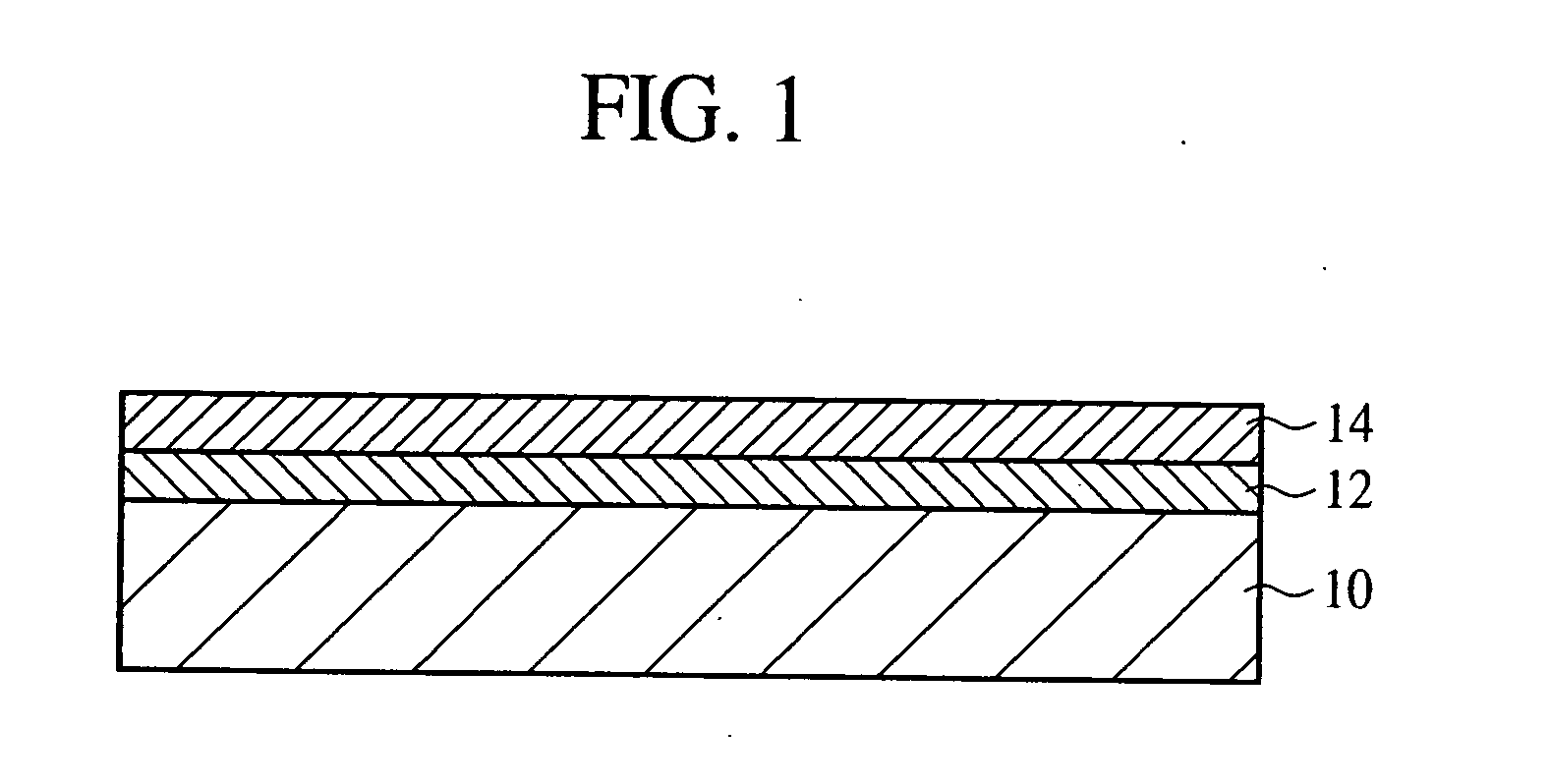
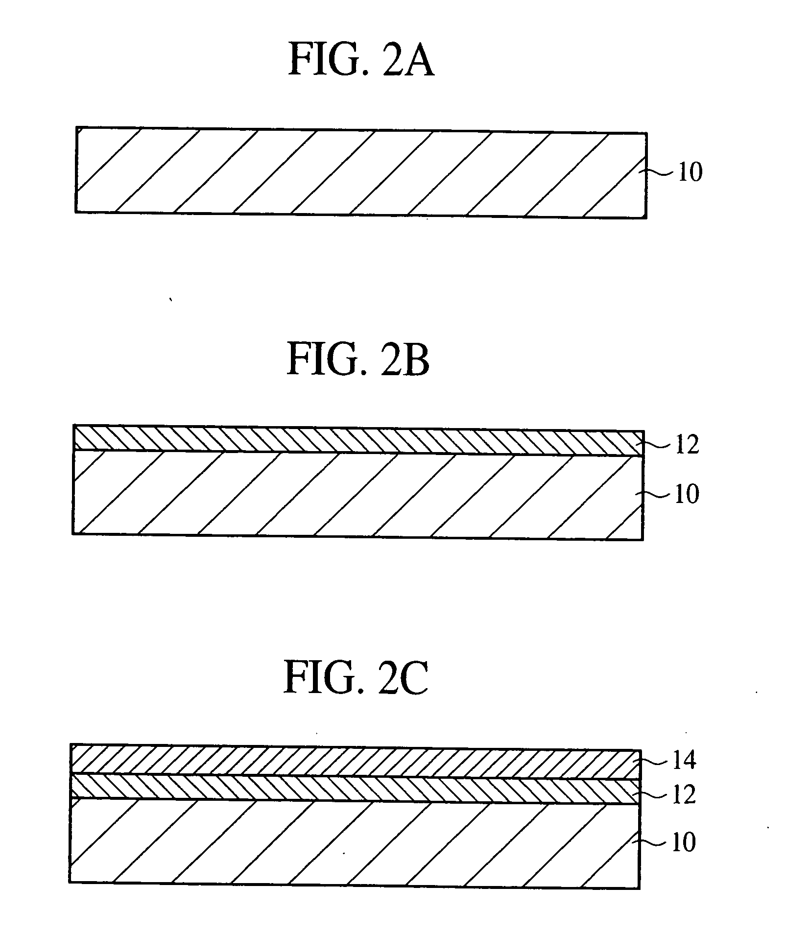
[0114] The semiconductor substrate according to a first embodiment of the present invention and the method for fabricating the semiconductor substrate will be explained with reference to FIGS. 1 to 2C. FIG. 1 is a sectional view of the semiconductor substrate according to the present embodiment.

[0115] (The Semiconductor Substrate)

[0116] First, the structure of the semiconductor substrate according to the present embodiment will be explained with reference to FIG. 1.

[0117] The semiconductor substrate according to the present embodiment is characterized mainly by a strained Si / SiGe structure having an isotope composition ratio of 28Si of a silicon crystal layer 14 set high.

[0118] As shown in FIG. 1, a 200 nm-thickness silicon germanium crystal layer 12 is epitaxially grown on the silicon crystal substrate 10. The silicon germanium crystal layer 12 has a composition of, e.g., Si0.7Ge0.3.

[0119] A 200 nm-thickness silicon crystal layer 14 is epitaxially grown on th...

second embodiment

A SECOND EMBODIMENT

[0138] The semiconductor substrate according to a second embodiment of the present invention and the method for fabricating the semiconductor substrate will be explained with reference to FIGS. 3 to 4C. FIG. 3 is a sectional view of the semiconductor substrate according to the present embodiment. The same members of the present embodiment as those of the semiconductor substrate and the method for fabricating the semiconductor substrate shown in FIGS. 1 to 2C are represented by the same reference numbers not to repeat or to simplify their explanation.

[0139] (The Semiconductor Substrate)

[0140] First, the semiconductor substrate according to the present embodiment will be explained with reference to FIG. 3.

[0141] The semiconductor substrate according to the present embodiment is characterized mainly by a strained Si / SiGe structure having 70Ge isotope composition ratio of a silicon germanium crystal layer 12a set high.

[0142] As shown in FIG. 3, the silicon germani...

third embodiment

A THIRD EMBODIMENT

[0153] The semiconductor substrate according to a third embodiment of the present invention and the method for fabricating the semiconductor substrate will be explained with reference to FIGS. 5 to 6C. FIG. 5 is a sectional view of the semiconductor substrate according to the present embodiment. The same members of the present embodiment as those of the semiconductor substrate and the method for fabricating the semiconductor substrate according to the first or the second embodiment shown in FIGS. 1 to 4C are represented by the same reference numbers not to repeat or to simplify their explanation

[0154] (The Semiconductor Substrate)

[0155] The semiconductor substrate according to the present embodiment will be explained with reference to FIG. 5.

[0156] The semiconductor substrate according to the present embodiment is characterized mainly by a strained Si / SiGe structure having a 70Ge isotope composition ratio of a silicon germanium crystal layer 12a set high and a 2...


PUM


Abstract

The semiconductor substrate comprises a silicon substrate 10, a silicon germanium layer 12 formed on the silicon substrate; and a silicon layer 14 formed on the silicon germanium layer. At least one of an isotope composition ratio of one Si isotope and an isotope composition ratio of a Ge isotope of at least one of the silicon substrate, the silicon germanium layer and the silicon layer is above 95%. In at least one of the silicon substrate, the silicon germanium layer and the silicon layer, at lest one of an isotope composition ratio of one Si isotope and an isotope composition ratio of one Ge isotope is set higher, whereby the heat can be scattered in the direction horizontal to the substrate plane. Thus, the semiconductor substrate can have higher heat radiation.

Description

CROSS-REFERENCE TO RELATED APPLICATION [0001] This application is based upon and claims priority of Japanese Patent Application No. 2002-192133, filed on Jul. 1, 2002, the contents being incorporated herein by reference. BACKGROUND OF THE INVENTION [0002] The present invention relates to a semiconductor substrate and a method for fabricating the semiconductor substrate, more specifically a semiconductor substrate which can improve heat radiation and a method for fabricating the semiconductor substrate. [0003] Improvements for higher speed have been continuously made on MOSFETs (Metal Oxide Semiconductor-Field Effect Transistors), etc. by micronizing elements, typically reducing the gate length. [0004] A propagation delay time τ of a signal in a MOSFET is expressed by the following formula. τ=Cload·Vdd / [{W·μ·ε) / (L·TOX)}×(Vdd−Vt)2]  (1) wherein Cload represents a load capacitance; Vdd represents a source voltage; W represents a gate width of the MOSFET; L represents a gate length of ...

Claims


Application Information

Patent Timeline
Patent Type & Authority Applications(United States)
IPC IPC(8): H01L21/02H01L21/20H01L21/205H01L21/336H01L21/762H01L21/84H01L27/12H01L29/04H01L29/10H01L29/161H01L29/165H01L29/78H01L29/786
CPCH01L21/02381H01L21/0245H01L21/02532H01L21/02609H01L21/02656H01L21/76254H01L29/78687H01L27/1203H01L29/045H01L29/1054H01L29/165H01L29/78603H01L21/84
Inventor FUKUDA, TETSUOHIRATA, KATSUSHI
Owner FUJITSU MICROELECTRONICS LTD
Learn More