
Class D amplifier

a class d amplifier and amplifier technology, applied in the direction of amplifiers, amplifiers with semiconductor devices only, amplifiers with semiconductor devices, etc., can solve the problems of waveform distortion in the output modulated signal, easy damage of transistors, and inability of class d amplifiers to perform predetermined operations, etc., to accurately detect excessive electric current flowing

Inactive Publication Date: 2006-02-09
PIONEER CORP
View PDF4 Cites 19 Cited by
  • Summary
  • Abstract
  • Description
  • Claims
  • Application Information

AI Technical Summary

Benefits of technology

[0031] Another object of the present invention is to provide a class D amplifier having excessive electric current detection means that can accurately detect excessive electric current flowing in switching elements that form a power amplification zone and operate in a push-pull manner.

Problems solved by technology

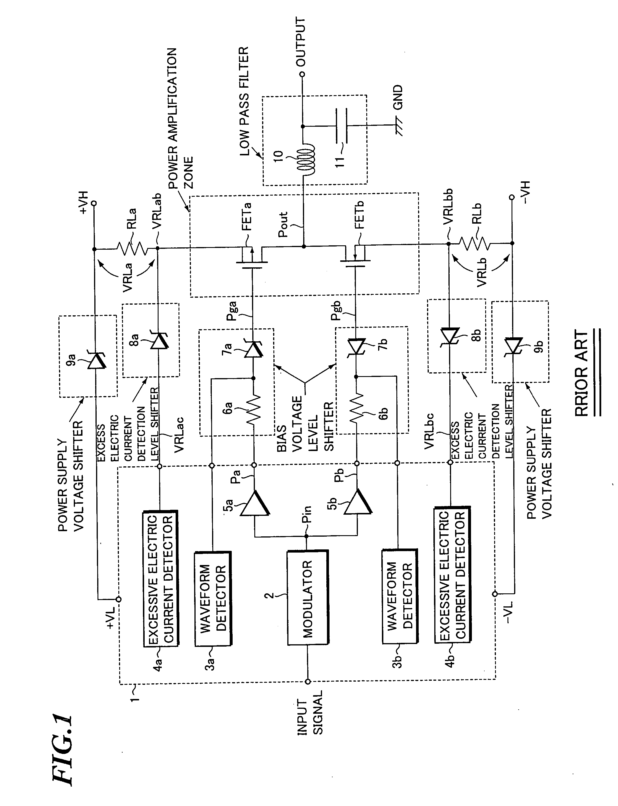
Since these Zener diodes 7a, 7b, 8a, 8b, 9a, 9b do not always generate equal Zener voltages for each set due to their electrical and other properties, there were problems of variations in the Zener voltages (manufacturing variations, fluctuations during operation, and the like), hence making it impossible for the class D amplifiers to perform the predetermined operations that are adjusted to the bias conditions described above.
As a result of the bias points of the drive signals Pga, Pgb shifting away from the correct bias, a load that exceeds the allowable power loss is applied to at least one of the transistors FETa and FETb, which leads to a problem of the transistors being easily damaged.
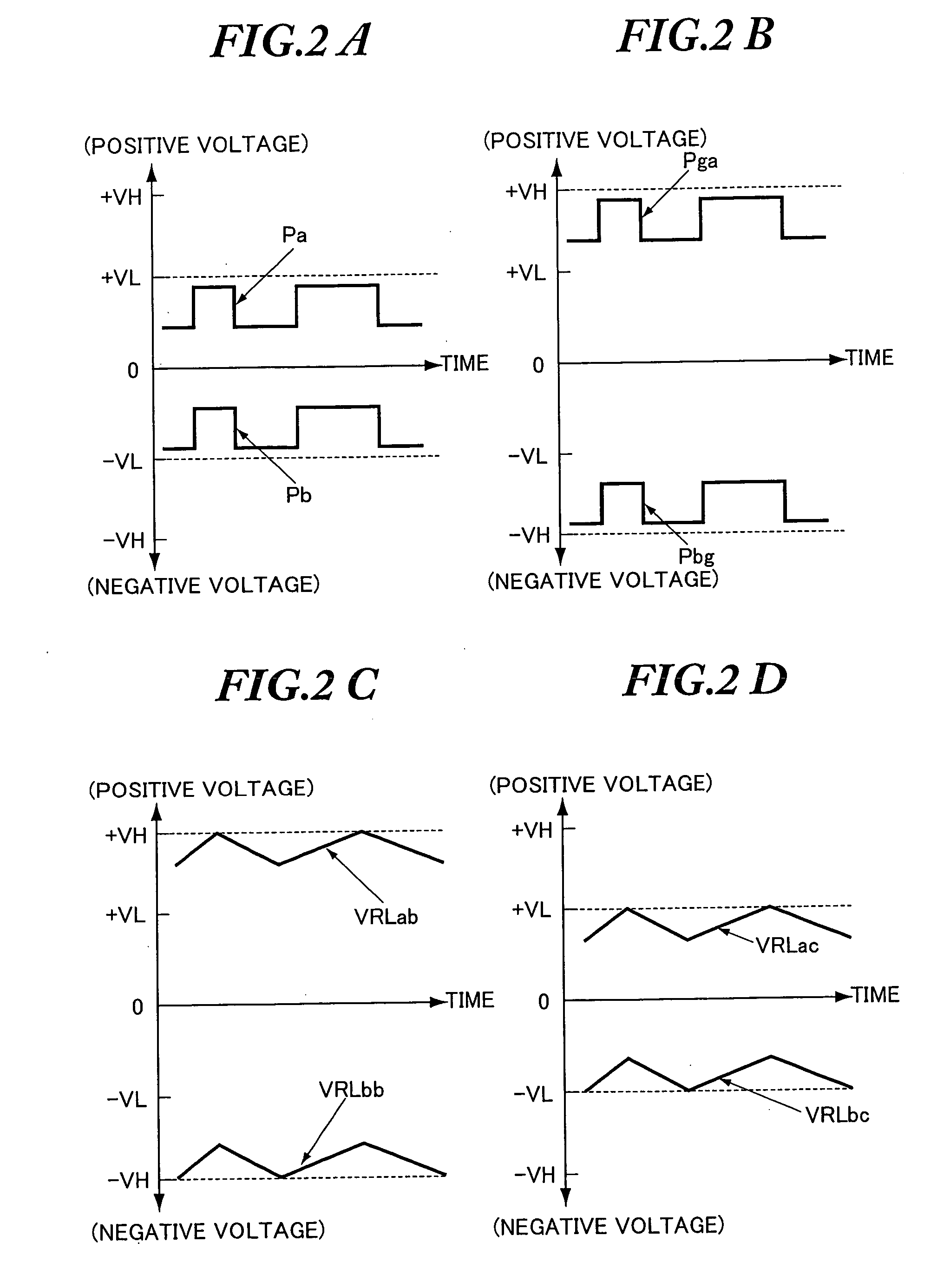
Even further, even if the Zener voltages of both the Zener diodes 7a and 7b are shifted from the correct Zener voltage, problems will occur such as waveform distortions in the output modulated signal Pout, inability to perform efficient power amplification, and damage to transistors FETa, FETb.
If variations occur in the Zener voltage of the Zener diode 8b that forms the excessive electric current detection level shifter of the positive power supply voltage −VH side, an offset voltage will be applied to the falling voltage VRLbc as illustrated in FIG. 2 (d), generating a voltage fluctuation and consequently causing a problem of the excessive electric current detector 4b not being able to correctly detect the excessive electric current flowing in the transistor FETb.
When variations in the Zener voltage occur in the Zener diodes 9a and 9b each forming a power supply voltage shifter, a problem occurs in which it becomes impossible to operate the semiconductor integrated circuit device 1 based on the correct voltage of two power supply voltages +VL and −VL.

Method used


Image

  • Class D amplifier
  • Class D amplifier
  • Class D amplifier

Examples


example

[0090] Next, a concrete example will be described in more detail with reference to FIG. 4 and FIG. 5.

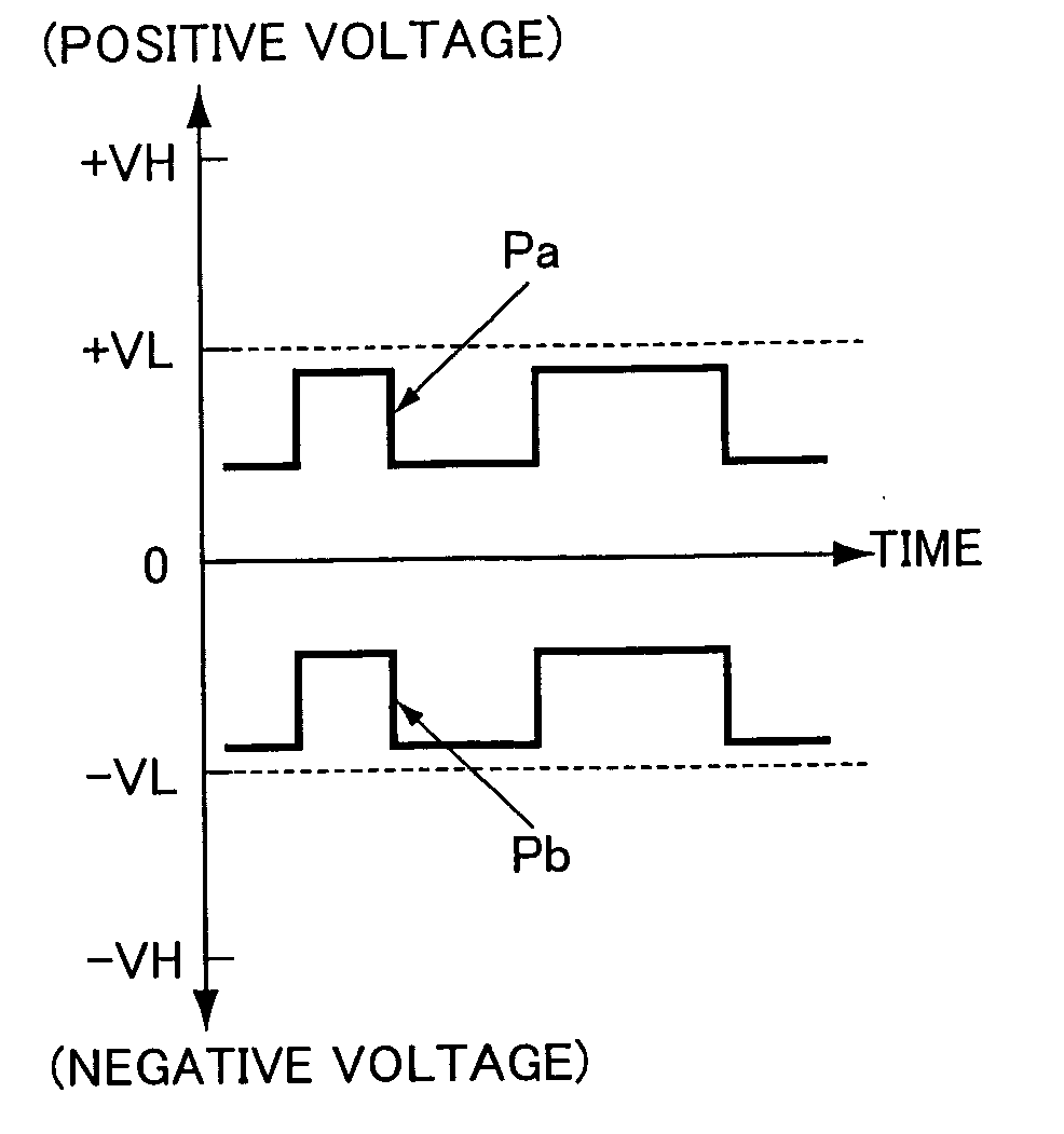
[0091]FIG. 4 is a schematic diagram showing the configuration of the class D amplifier 100 of the example. Parts identical or equivalent to those showing in FIG. 3 are denoted by the same symbols. FIG. 5 describes the operation of the class D amplifier 100 of this example. In particular, FIGS. 5(a) and 5(b) describe the operation of the bias voltage level shifters 102a and 102b (described later) and FIG. 5(c) describes the operation of the current mirror circuits 101A and 101B which serve as excessive electric current detection means (described later).

[0092] In the following the characteristic parts of the configuration of the class D amplifier 100 in this example is described compared with the class D amplifier according to the embodiment shown in FIG. 3.

[0093] The bias voltage level shifter 102a provided in the class D amplifier 100 of this example comprises resistors R1a and R2...


PUM


Abstract

A drive signal that matches the bias of a transistor is generated. A differential amplifier calculates the difference between a specified voltage of negative power supply and another input signal. Then, a resistor that realizes a pull-down function level-shifts it towards a negative power supply voltage having a higher absolute voltage value to generate another differential signal, which is in turn amplified in another amplifier, to generate another drive signal that matches the bias of another transistor. Respective current mirror circuits detect a falling voltage occurring at both ends of a resistor connected between the transistor and the higher positive power supply voltage and a falling voltage occurring at both ends of a resistor connected between the other transistor and the higher negative power supply voltage, respectively. Then, the presence of an excessive electric current is detected by generating electric currents in accordance with to the falling voltages.

Description

BACKGROUND OF THE INVENTION [0001] The present invention relates to a class D amplifier that amplifies square-wave signals which have undergone, for example, pulse width modulation (PWM) or pulse density modulation (PDM). [0002] The present application claims priority from Japanese Application No. 2004-226928, the disclosure of which is incorporated herein by reference. [0003] In recent years, simpler, smaller, and higher efficiency system configurations of audio systems performing digital signal processing have been strived for through the use of class D amplifiers. In these systems, the class D amplifiers amplify square-wave audio signals (so-called, 1-bit stream format audio signals) formed by pulse width modulation or pulse density modulation and directly supply them to speakers via a low-pass filter. [0004]FIG. 1 is a schematic diagram that represents the configuration of a conventional class D amplifier applied to this type of digital audio system. [0005] The class D amplifier...

Claims


Application Information

Patent Timeline
IPC IPC(8): H03F3/217
CPCH03F3/217
Inventor OZAWA, AKIOKUDO, KAZUYUKI
Owner PIONEER CORP
Learn More