

Method of electric field assisted deposition of films of nanoparticles
- Summary
- Abstract
- Description
- Claims
- Application Information
AI Technical Summary
Benefits of technology
Problems solved by technology
Method used
Image

Examples
Embodiment Construction
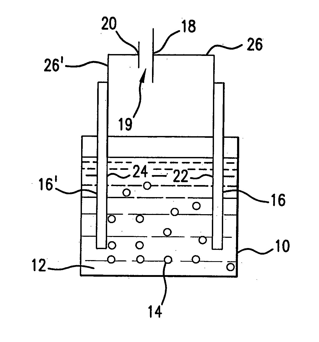
[0035] Referring to FIG. 1, there is shown a schematic diagram of an apparatus for carrying out an exemplary embodiment of the method of the present invention for forming nanoparticle films. The apparatus comprises a vessel 10 containing a substantially non-conducting nonpolar solvent 12 having ligand-capped nanoparticles 14 suspended therein. In the present embodiment, the solvent 12 is hexane and the nanoparticles 14 are nanocrystals of CdSe having a mean diameter of from about 3 nm to about 4 nm, where each nanoparticle has trioctylphosphine (TOP) ligands and / or trioctylphosphine oxide (TOPO) ligands attached thereto. When capped with TOP ligands and / or TOPO ligands, these nanoparticles are commonly termed “TOPO-capped CdSe nanocrystals.” CdSe nanocrystals useful in the method of the present invention may be prepared according to the methods described in Murray et al., J. Am. Chem. Soc. 115, 8706 (1993), which is hereby incorporated by reference in its entirety. The concentration...
PUM
| Property | Measurement | Unit |
|---|---|---|
| Thickness | aaaaa | aaaaa |
| Thickness | aaaaa | aaaaa |
| Size | aaaaa | aaaaa |
Abstract
Description
Claims
Application Information