Organic electronic device and process forming the same

Inactive Publication Date: 2006-02-16
EI DU PONT DE NEMOURS & CO
View PDF18 Cites 12 Cited by
  • Summary
  • Abstract
  • Description
  • Claims
  • Application Information

AI Technical Summary

Benefits of technology

[0073] In the OLED embodiment, the invention can provide static brightness (shading) bias or color bias in the context of a passive matrix display. For example, the invention can be used to provide a darker (or lighter) icon image as part of, or the whole of an organic light emitting diode display.
[0074] In one embodiment, the invention can also provide brightness (shading) bias or color bias in the context of an active matrix display. For example, the invention can be used to provide one or more display areas that are always darker (or lighter) than other areas of the display (windowing). For instance, less important information can be displayed in a darker surrounding area while more important information can be displayed in a brighter island (window) area. It is important to note that these brightness biased areas may or may not contain addressed cells (e.g., pixels). This implementation of the invention can provide a significant advantage via cost savings with regard to both fabrication and operation by obviating the need for brightness or color bias addressing circuitry.
[0075] In one embodiment, the invention can provide large size displays with high information content, with the significant advantage that these same displays can be

Problems solved by technology

This two-states (on or off) constraint limits the resolution and the quality of the image.
Again, the two-states constraint limits the resolution and the quality of the image.
Howeve

Method used


Image

  • Organic electronic device and process forming the same
  • Organic electronic device and process forming the same

Examples


example 1

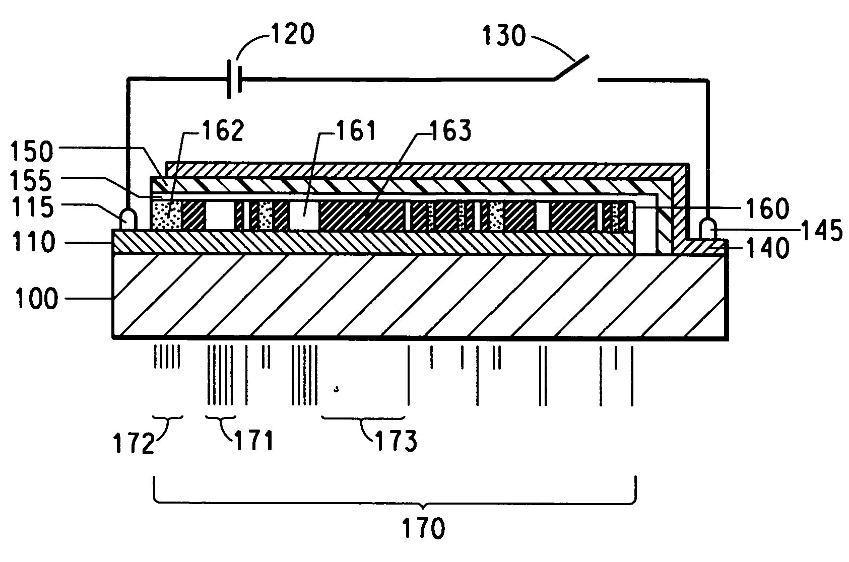
[0078] This Example demonstrates selective exposure of an organic resistive layer to varying amounts of a chemical to fabricate a static gray-scale organic light emitting diode array. The result is a device including an organic resistive layer defining a plurality of ionic regions where each of at least three regions are characterized by one of at least three compositions corresponding to discrete resistances that are different from one another.

[0079] Referring to FIG. 1, the substrate 100 is 30×30 mm (nominal) glass and the first electrode 110 is indium tin oxide. The organic resistive layer 160 in this experiment is formed by spin-coating a polyaniline layer. Portions of the spin-coated polyaniline that will not form any of the regions 161, 162, 163 are removed by laser ablation. An ink jet head exposes the second region 162 and the third region 163 of the polyaniline to two different ratios of acetone to propanol, while not exposing the first region 161. The organic resistive la...

example 2

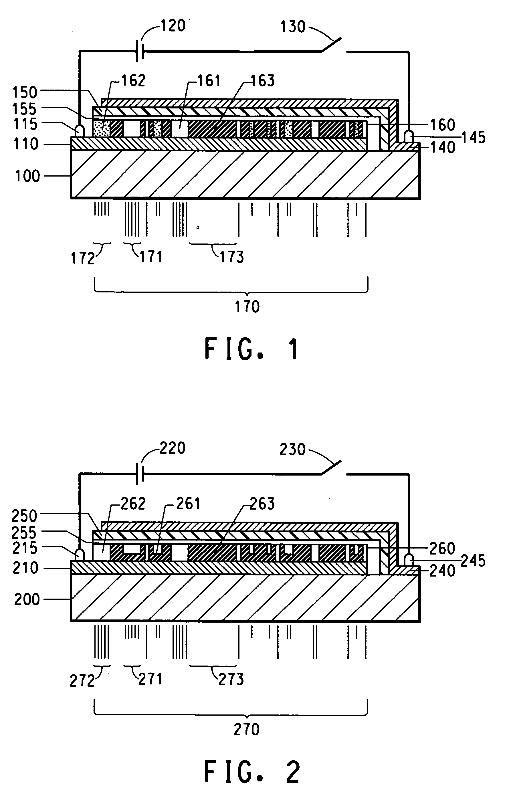
[0080] This Example demonstrates selective removal of varying amounts of an organic resistive layer to fabricate an organic light emitting diode array. The result is a device including an organic resistive layer defining a plurality of ohmic regions where each of at least three regions are characterized by one of at least three thicknesses that correspond to discrete resistances that are different from one another.

[0081] Referring to FIG. 2, the substrate 200 is 30×30 mm (nominal) glass and the anode 210 is indium tin oxide. The organic resistive layer 260 in this experiment is formed by screen printing a carbon / phenolic resistor paste onto the indium tin oxide followed by curing at approximately 150° C. The cured paste is then covered with a lithographic mask having a first set of apertures over the second regions 262 and dry etched to an initial depth. A second set of apertures is then opened in the mask over the first regions 261 and the cured paste in the first regions 261 and ...

example 3

[0082] This Example demonstrates selective blending of varying amounts of components to define an organic resistive layer to fabricate a static gray-scale organic light emitting diode array. The result is a device including an organic resistive layer defining a plurality of electronic regions where each of at least three regions are characterized by one of at least three compositions corresponding to discrete resistances that are different from one another.

[0083] Referring to FIG. 1, the substrate 100 is 30×30 mm (nominal) glass and the first electrode 110 is indium tin oxide. The organic resistive layer 160 in this experiment is formed by ink jet printing a range of blended compositions. An ink jet head prints the first region 161, the second region 162 and the third region 163 using three different ratios of polyaniline to poly(3,4-ethylenedioxythiophene) to tetrathiafulvalene tetracyanoquinodimethane. The portions of the organic resistive layer that will not form any of the regi...


PUM

PropertyMeasurementUnit
Thicknessaaaaaaaaaa
Electrical resistanceaaaaaaaaaa
Areaaaaaaaaaaa

Abstract

An organic electronic device includes a first electrode layer, an organic resistive layer coupled to the first electrode layer wherein the organic resistive layer defines at least three regions, an organic active layer coupled to the organic resistive layer, and a second electrode layer coupled to the organic active layer. Each of the at least three regions is characterized by one of the plurality of resistances and the plurality of resistances includes at least three discrete resistances that are different from one another. The regions can be fabricated by selectively exposing portions of the organic resistive layer to a chemical, selectively removing portions of the organic resistive layer, or depositing a plurality of blends.

Description

FIELD OF THE INVENTION [0001] The invention relates generally to organic electronic devices and methods for forming organic electronic devices. BACKGROUND INFORMATION [0002] Organic electronic devices have attracted increasing attention in recent years. Examples of organic electronic devices include organic light emitting diodes (“OLEDs”). A typical OLED includes an electroluminescent organic active layer between two electrodes, where at least one of the electrodes is transparent. [0003] Static graphic displays using organic light emitting diode arrays have been constructed by patterning one of the electrode layers. In this approach, a transparent indium tin oxide layer electrode has been patterned. However, in this approach, the patterned electrode display permits only two states (i.e., on or off) based on whether the electrode is present or absent across an area of interest. This two-states (on or off) constraint limits the resolution and the quality of the image. [0004] Organic l...

Claims


Application Information

Patent Timeline
IPC IPC(8): H05B33/00
CPCH01L27/3239H01L2251/558H01L51/5088Y10S428/917H10K59/221H10K50/17H10K2102/351
Inventor YU, GANGTRUONG, NUGENT
Owner EI DU PONT DE NEMOURS & CO
Why Eureka
Try Eureka