Laser processing method

a laser processing and laser technology, applied in the field of laser processing methods, can solve the problems of reducing productivity, reducing and large area ratio of dividing lines to wafers, and achieve the effect of increasing the processing depth of laser grooves

Inactive Publication Date: 2006-02-16
DISCO CORP
View PDF14 Cites 22 Cited by
  • Summary
  • Abstract
  • Description
  • Claims
  • Application Information

AI Technical Summary

Benefits of technology

[0006] It is an object of the present invention to provide a laser processing method capable of increasing a processing depth of a laser groove formed by one time of laser processing and carrying out processing without accumulating debris produced by the application of a laser beam in a groove having been formed by laser processing.

Problems solved by technology

Since the cutting blade has a thickness of about 20 μm, however, the dividing lines for sectioning chips must have a width of about 50 μm and hence, the area ratio of the dividing lines to the wafer is large, thereby reducing productivity.
Further, since a sapphire substrate, silicon carbide substrate and the like have high Mohs hardness, cutting with the above cutting blade is not always easy.
Consequently, problems arise in that a laser beam applied next is cut off or the focusing spot of the laser beam cannot be set to the bottom of the laser groove, thereby making it impossible to form laser grooves having a predetermined depth efficiently.

Method used


Image

  • Laser processing method
  • Laser processing method
  • Laser processing method

Examples


Embodiment Construction

[0027] The laser processing method of the present invention will be described in more detail hereinunder with reference to the accompanying drawings.

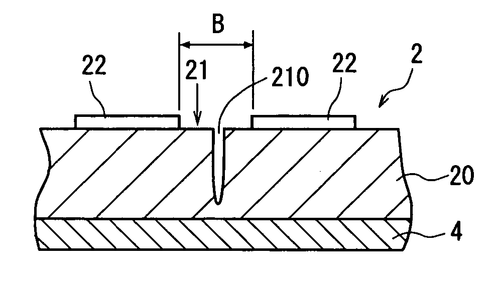
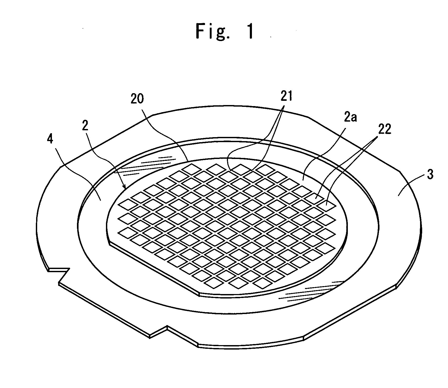
[0028]FIG. 1 is a perspective view of a semiconductor wafer as a workpiece to be processed by the laser processing method of the present invention. In the semiconductor wafer 2 shown in FIG. 1, a plurality of areas are sectioned by a plurality of dividing lines 21 arranged in a lattice pattern on the front surface 20a of a semiconductor substrate 20 such as a GaAs substrate and a device 22 such as IC or LSI is formed in each of the sectioned areas. A back surface of the thus constituted semiconductor wafer 2 is put on a protective tape 4 mounted on an annular frame 3 in such a manner that the front surface 2a, that is, the surface, on which the dividing line 21 and device 22 are formed, faces up.

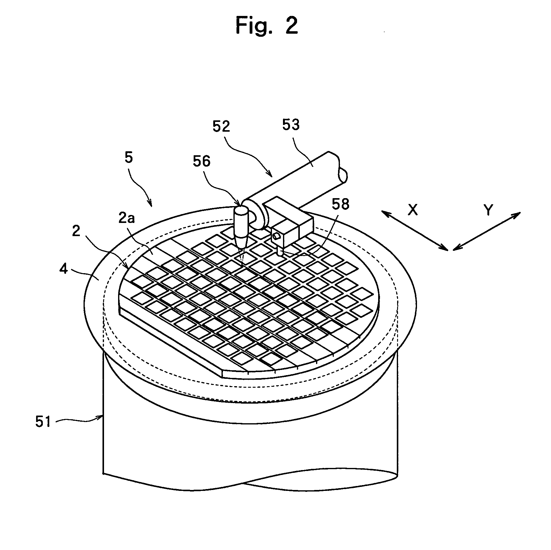
[0029] FIGS. 2 to 4 show a laser beam processing machine for carrying out the laser processing method of the present invention. The laser pro...


PUM

PropertyMeasurementUnit
diameteraaaaaaaaaa
diameteraaaaaaaaaa
widthaaaaaaaaaa

Abstract

A laser processing method for forming a laser groove along dividing lines by applying a pulse laser beam along the dividing lines formed on a workpiece, the method comprising the steps of forming the focusing spot of the pulse laser beam in a shape of oval, positioning the long axis of the oval focusing spot along each of the dividing lines, and moving the focusing spot and the workpiece along the dividing line relative to each other.

Description

FIELD OF THE INVENTION [0001] The present invention relates to a method of carrying out laser processing along dividing lines called “streets formed on a workpiece such as a semiconductor wafer or the like. DESCRIPTION OF THE PRIOR ART [0002] In the production process of a semiconductor device, a plurality of areas are sectioned by dividing lines called “streets” arranged in a lattice pattern on the front surface of a substantially disk-like semiconductor wafer, and a circuit (function element) such as IC or LSI is formed in each of the sectioned areas. Individual semiconductor chips are manufactured by cutting this semiconductor wafer along the dividing lines to divide it into areas having the circuit formed thereon. An optical device wafer comprising light-receiving elements (function elements) such as photodiodes or light emitting elements (function elements) such as laser diodes laminated on the front surface of a sapphire substrate is also cut along dividing lines to be divided...

Claims


Application Information

Patent Timeline
Patent Type & Authority Applications(United States)
IPC IPC(8): H01L21/50B23K26/06B23K26/073B23K26/364B23K26/38B23K26/40B23K101/40H01L21/301
CPCB23K26/063B23K26/0736H01L21/78B23K26/4075B23K26/367B23K26/40B23K26/0622B23K26/364B23K2103/50
Inventor OBA, RYUGOFURUTA, KENJIHOSHINO, HITOSHIKITAHARA, NOBUYASUTAKEDA, NOBORU
Owner DISCO CORP
Why Eureka
Try Eureka