Method for manufaturing semiconductor device and substrate processing system

a processing system and semiconductor technology, applied in the direction of coatings, chemical vapor deposition coatings, metallic material coating processes, etc., can solve the problems of increasing the cost accordingly and the inability to improve the output, and achieves the effect of improving controllability, convenient execution and convenient execution

Inactive Publication Date: 2006-02-16
KOKUSA ELECTRIC CO LTD
View PDF8 Cites 25 Cited by
  • Summary
  • Abstract
  • Description
  • Claims
  • Application Information

AI Technical Summary

Benefits of technology

[0040] In a seventh aspect, the substrate processing apparatus according to the fifth aspect is provided, wherein the controller further has a function to make the flow rate of the liquid source to the vaporization section per one injecting operation smaller than the flow rate corresponding to one supplying operation of the source gas obtained by vaporizing in the vaporization section to the substrate, and control the flow rate by the number of injection. When the controller has such a function, the method of manufacturing the semiconductor device of the third aspect can be easily executed.
[0041] In an eighth aspect, the substrate processing apparatus according to the fifth aspect is provided, wherein the controller further has a function to control so as to deposit on the substrate by using an ALD, by repeating for a plurality of times a step of supplying one reactant to the substrate to be adsorbed thereon, and a step of forming a film by supplying other reactant to the reactant already adsorbed on the substrate so as to be reacted thereon. When the controller has such a function, the method of manufacturing the semiconductor device of the fourth aspect can be easily executed.
[0042] In a ninth aspect, the substrate processing apparatus according to the fifth aspect is provided, wherein the controller further has a function to previously measure the correlation between a pressure for feeding the liquid source to the vaporization section and the flow rate per one injecting operation, and correct the flow rate per one injecting operation based on the correlation thus obtained. When the controller has a function to correct the flow rate based on the correlation between the pressure and the flow rate, the flow rate per one injecting operation to the vaporization section can be fixed without being affected by the change of pressure.
[0043] In a tenth aspect, the substrate processing apparatus according to the fifth aspect is provided, wherein a liquid flow meter is provided between the vaporization section and the container, and an injection drive control mechanism having a flow rate adjusting mechanism electrically connected to the liquid flow meter is installed, and the flow rate adjusting mechanism has a controller that calculates an integrated flow rate of a certain time period or a certain constant number of injection based on an electrical signal from the liquid flow meter, monitors the integrated flow rate thus obtained with passage of time, and adjusts a change in the flow rate to the vaporization section per one injecting operation with passage of time. When the controller has a function to adjust the change of the flow rate with passage of time per one injecting operation to the vaporization section, the flow rate per one injecting operation to the vaporization section can be fixed, without being influenced by the change of the injection drive contr

Problems solved by technology

Therefore, the number of injection is increased compared with the CVD method and the MOCVD method, thus posing a problem that a throughput can not be improved.
Ther

Method used


Image

  • Method for manufaturing semiconductor device and substrate processing system
  • Method for manufaturing semiconductor device and substrate processing system
  • Method for manufaturing semiconductor device and substrate processing system

Examples


Embodiment Construction

[0063] Embodiments of the present invention will be explained hereafter.

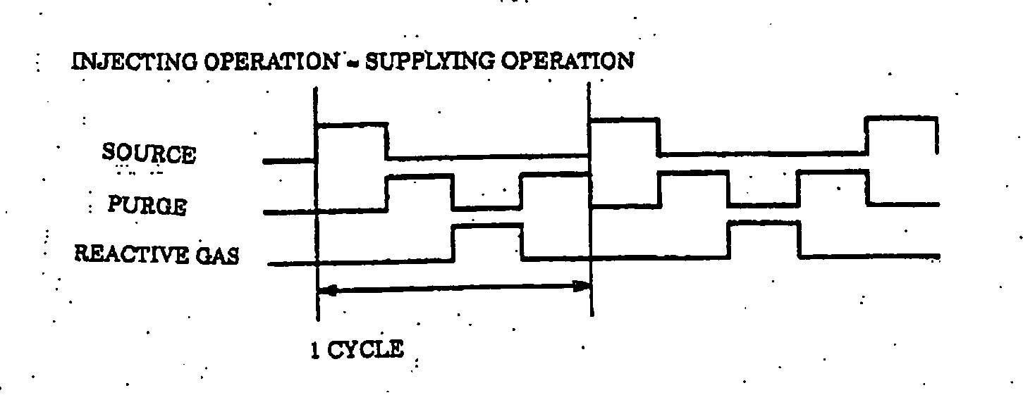
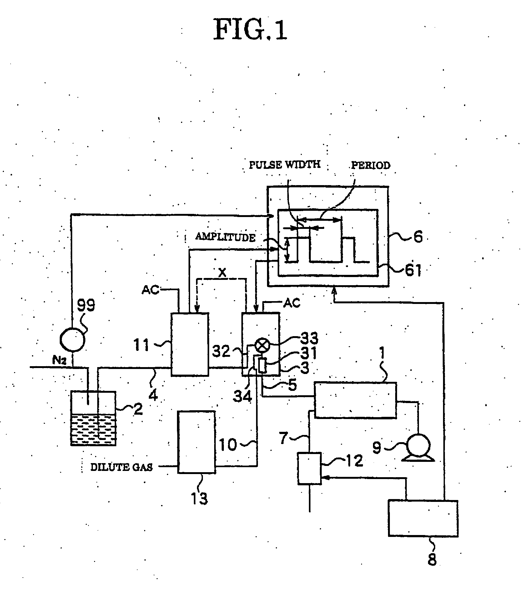
[0064]FIG. 1 is a block diagram of a device for performing a method of manufacturing a semiconductor device, which is an example of a substrate processing apparatus, wherein a liquid law material vaporizing system is adopted. The method of manufacturing the semiconductor device adopted by this substrate processing apparatus comprises: [0065] supplying one reactant on a substrate; [0066] supplying other reactant to the substrate; and [0067] processing the substrate by repeating the above steps for a plurality of times.

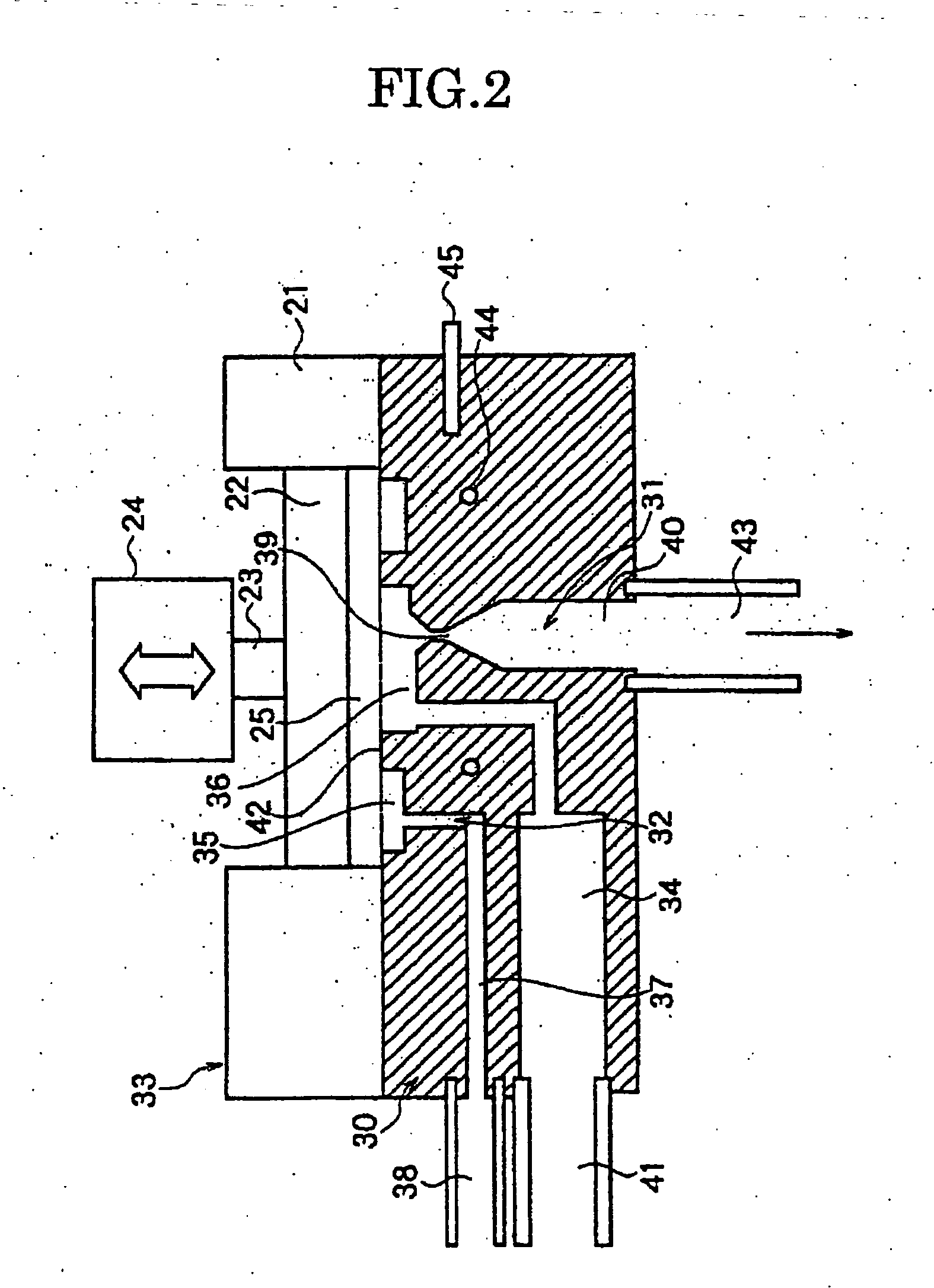
[0068] The substrate processing apparatus comprises a processing chamber 1, a source container 2, a vaporizer 3, a liquid source supply pipe 4, a source gas supply pipe 5, an injection drive control mechanism 6, a reactive gas supply pipe 7, and a controller 8.

[0069] The processing chamber 1 is constituted so that a substrate may be processed internally, and connected to a pump 9 so as to be exha...


PUM

PropertyMeasurementUnit
Thicknessaaaaaaaaaa
Pressureaaaaaaaaaa
Flow rateaaaaaaaaaa

Abstract

To improve throughput of a substrate processing without wastefully using a source as a reactant by repeating supply steps of a plurality of reactants for a plurality of times. A substrate processing apparatus includes a source gas obtained by vaporizing a liquid source as a reactant, and functions to process a substrate by repeating the supply of the source gas into a processing chamber 1, and the supply of the reactant different from the source gas into the processing chamber 1, which is executed subsequently, for a plurality of times. A flow rate of the liquid source is controlled by an injection drive control mechanism 6. The injection drive control mechanism 6 is designed to fix the flow rate per one injecting operation of the liquid source directly flowing into a vaporization section in a vaporizer 3, and intermittently inject the liquid source to a vaporization section 31.

Description

TECHNICAL FIELD [0001] The present invention relates to a manufacturing method of a semiconductor device and a substrate processing apparatus, particularly to the substrate processing apparatus for processing the substrate by using a reaction product containing a source gas obtained by vaporizing a liquid source. BACKGROUND ART [0002] Generally, a substrate processing apparatus for manufacturing a semiconductor device which processes the substrate by using a liquid source requires a liquid source vaporizing system for vaporizing the liquid source. The gas (referred to as vaporized gas hereafter) vaporized by increasing the temperature of the liquid source in the liquid source vaporizing system must be prevented from being liquefied at a high temperature. Therefore, piping has to be heated if needed. Particularly, a source in a gas state of vaporized metal has a low vapor pressure and is liquefied by being cooled by piping. Therefore, the piping needs to be heated. In order to proces...

Claims


Application Information

Patent Timeline
IPC IPC(8): H01L21/469C23C16/00C23C16/40
CPCC23C16/405C23C16/45527C23C16/4486
Inventor HORII, SADAYOSHIMIYA, HIRONOBU
Owner KOKUSA ELECTRIC CO LTD
Why Eureka
Try Eureka