Optoelectronic conversion header, LSI package with interface module, method of manufacturing optoelectronic conversion header, and optical interconnection system

a technology of optoelectronic conversion and interface module, which is applied in the direction of optical waveguide light guide, instruments, optics, etc., can solve the problems of easy damage to optical semiconductor devices, easy generation of so-called external optical feedback noise, and insufficient improvement of printed wiring board mounting lsi to achieve a sufficiently high signal transfer rate, the effect of simple structure and low cos

Active Publication Date: 2006-02-23
KK TOSHIBA
View PDF13 Cites 76 Cited by
  • Summary
  • Abstract
  • Description
  • Claims
  • Application Information

AI Technical Summary

Benefits of technology

[0012] It is an object of the present invention to provide, at low cost and with high performance, an optoelectronic conversion header, an LSI package with an interface module using the optoelectronic conversion heade...

Problems solved by technology

However, even though the processing speed is improved in the LSI, a printed wiring board mounting the LSI is not so sufficiently improved as to have a sufficiently high signal transfer rate or speed for transferring a signal from the high speed processing LSI.
The conventional structure disclosed in Jpn. Pat. Appln. KOKAI Publication No. 2000-347072 has a problem that if the optical fiber is inserted in a support member provided with the surface emitting laser to optically couple the surface emitting laser to the optical fiber for assembly of the structure, the optical fiber contacts an active area of the optical semiconductor device and this contact easily damage the optical semiconductor device.
There is also a problem that since the surface emitting laser is proximately disposed in parallel with the optical fiber, the external feedback light rays are input to the surface emitting laser and easily generate so-called external optical feedback noise.
However, there is a problem in which a temperature change easily varies an inclination angle of the optical semiconductor device in this structure that is provide with the metal projections having different heights or the block having the inclined plane to obliquely dispose the optical semiconductor device.
Another problem is the excessively low optical coupling efficiency between the surface emitting laser and the optical fiber resulting from the excessive setting of the inclination angle of the optical semiconductor device.
Moreover, the conventional structure in ...

Method used


Image

  • Optoelectronic conversion header, LSI package with interface module, method of manufacturing optoelectronic conversion header, and optical interconnection system
  • Optoelectronic conversion header, LSI package with interface module, method of manufacturing optoelectronic conversion header, and optical interconnection system
  • Optoelectronic conversion header, LSI package with interface module, method of manufacturing optoelectronic conversion header, and optical interconnection system

Examples


first embodiment

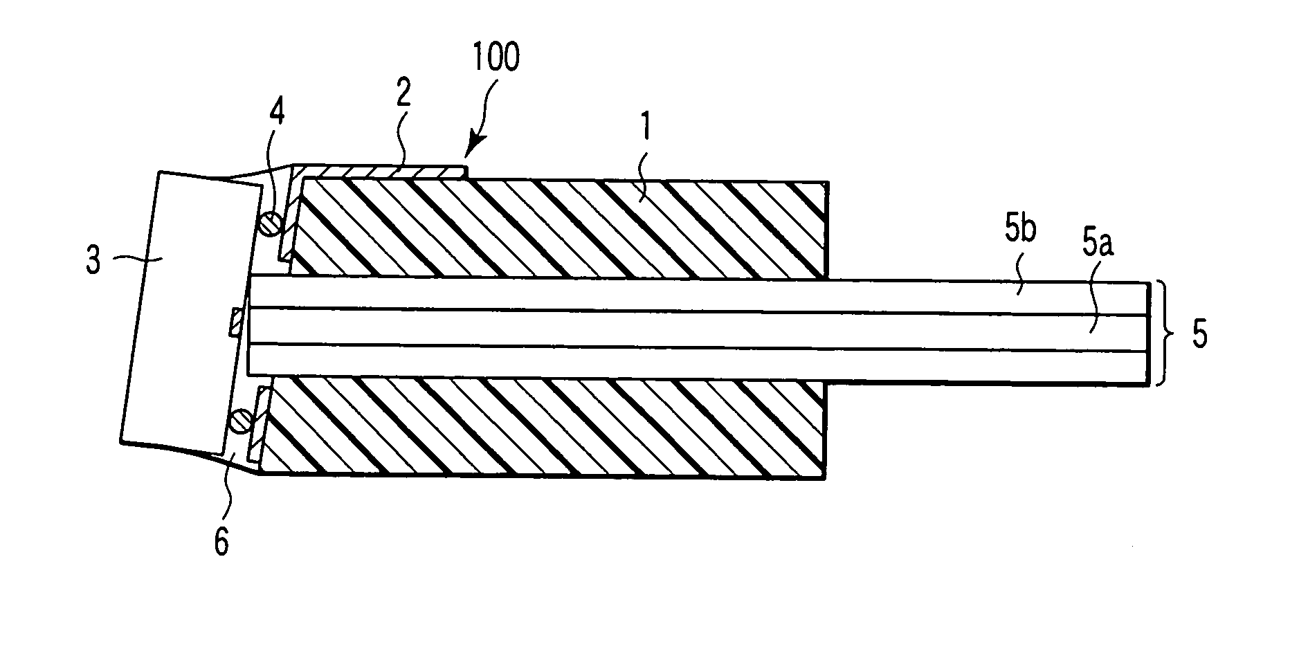
[0090]FIG. 2 is a sectional view schematically showing an optoelectronic conversion header 100 at a transmitting side according to a first embodiment of the present invention.

[0091] In the optoelectronic conversion header 100 at the transmitting side shown in FIG. 2, an optical fiber 5 is held by a ferrule 1, which serves as an optical waveguide to guide an optical signal. The optical waveguide is not limited to the optical fiber 5, and may be an optical waveguide film. The optoelectronic conversion header 100 in which the optical fiber 5 is held by the ferrule 1 will be described below. The optical fiber 5 is inserted into an insertion hole formed in the ferrule 1, and this ferrule 1 aligns an end face of the optical fiber 5 with a surface light emitter 3 such as a vertical cavity surface emitting laser (VCSEL). Thus, the optical signal guided via a core 5A of the optical fiber 5 is emitted from its end face to a light-emitting portion of the light emitter 3. It is to be noted in ...

second embodiment

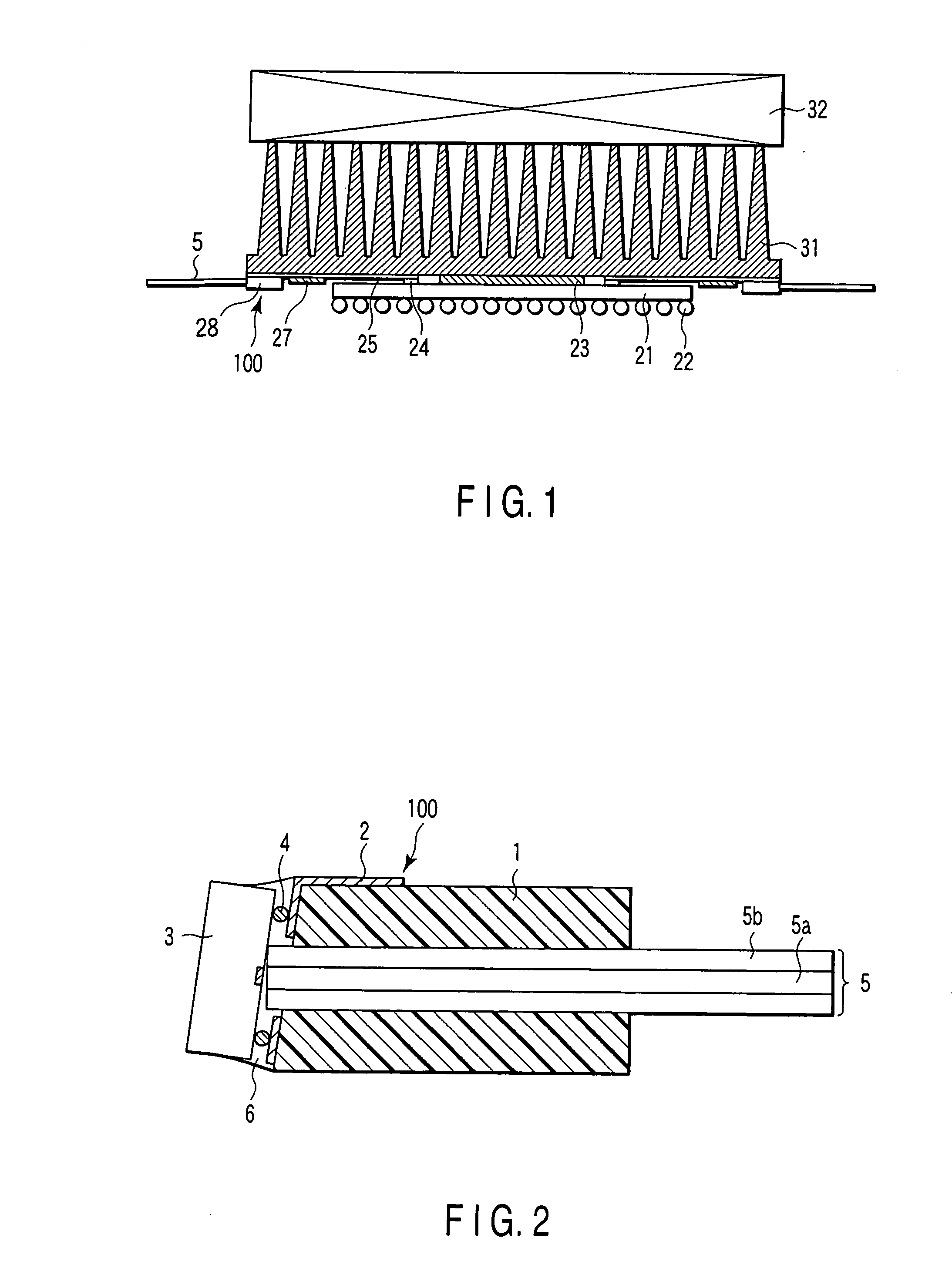
[0130]FIG. 7A is a plan view schematically showing a light emitter as an optical semiconductor device mounted on an optoelectronic conversion header 100 at a transmitting end according to a second embodiment of the present invention, and FIG. 7B is a sectional view along the VII-VII line shown in FIG. 7A. FIG. 8A is a also plan view schematically showing a photo detector as an optical semiconductor device mounted on the optoelectronic conversion header 100 at a receiving end according to the second embodiment of the present invention, and FIG. 8B is a sectional view along the VIII-VIII line shown in FIG. 8A. A structure of the optical semiconductor device itself may be of a mesa type such as that of the VCSEL described above, but a type of device with low electrode capacitance is shown here by way of example for the purpose of high-speed operation.

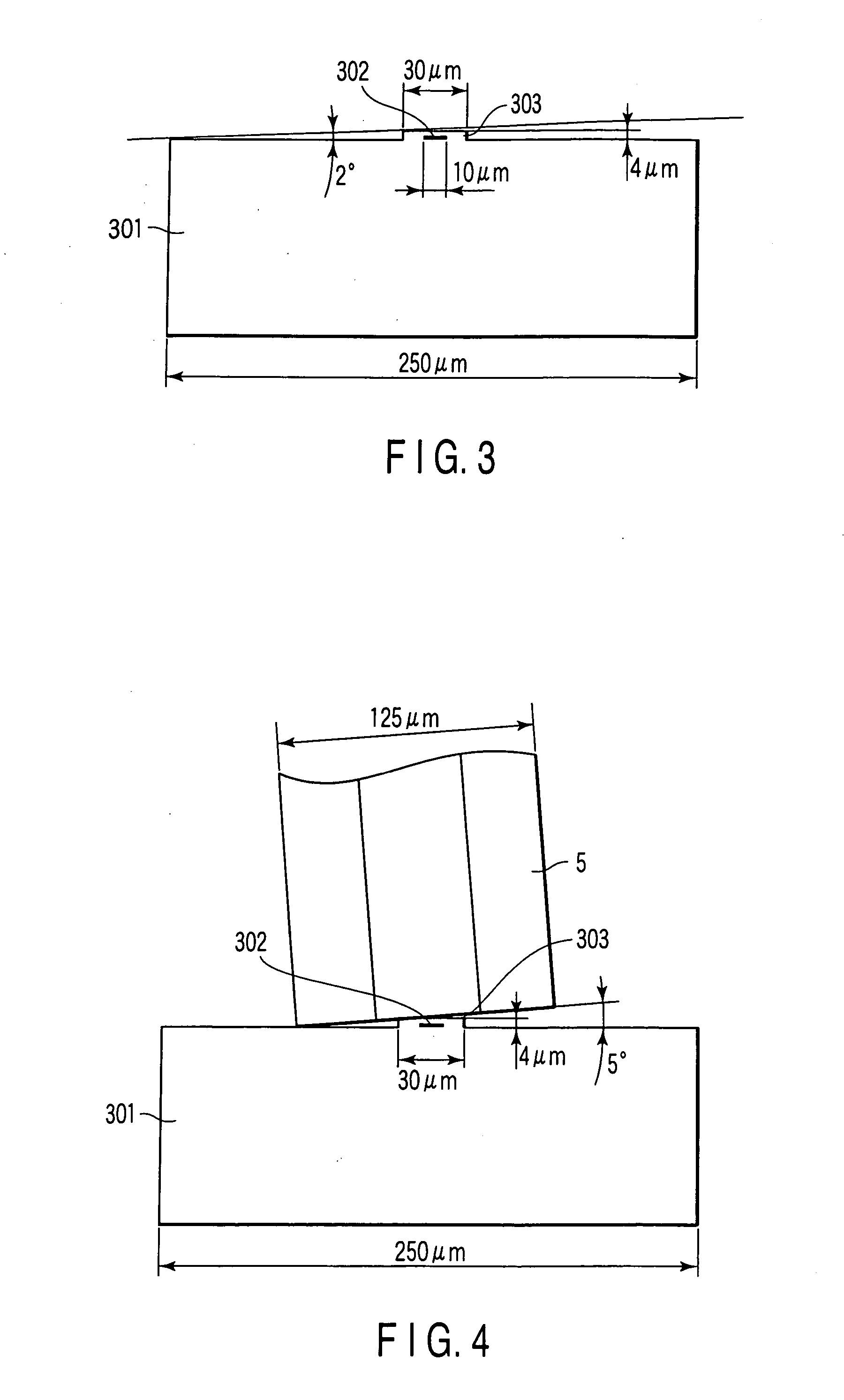
[0131] In FIG. 7A and FIG. 7B, a numeral 301 denotes a semiconductor substrate, a numeral 302 denotes a laser oscillation area where a l...

third embodiment

[0137]FIG. 10 is a sectional view schematically showing an optoelectronic conversion header 100 according to a third embodiment of the present invention. It is to be noted that the same numerals are assigned to the same parts as those in FIG. 2, and these are not described in detail.

[0138] A structure shown in FIG. 10 is built in such a manner that a light absorbing resin 8 is additionally provided in the structure shown in FIG. 2. A light absorbing resin 8 includes, for example, carbon fine particles, a pigment material, or epoxy resin, acrylic resin or silicone resin into which germanium fine particles are mixed, and is formed into a shape as shown in FIG. 10 by, for example, a resin mold. In this connection, it is preferable that the light absorbing resin 8 be provided to have a thickness which makes it sufficiently opaque for a wavelength used, for example, a thickness of 0.5 mm when a wavelength is 850 nm and the resin contains the Ge particles at 20%, and the light absorbing ...


PUM


Abstract

In an optoelectronic conversion header, a ferrule holds an optical waveguide in a predetermined position so that an end face of the optical waveguide protrudes from an mounting surface of the ferrule. An electric wire is provided on the mounting surface of the ferrule, a optical semiconductor device is mounted on the mounting surface of the ferrule and electrically connected to the electric wire. From the end face of the optical waveguide, an optical signal is transferred in a transfer direction and the mounting surface of the ferrule is so arranged as to be deviated two degrees or more from a plane vertical to the transfer direction.

Description

CROSS-REFERENCE TO RELATED APPLICATIONS [0001] This application is based upon and claims the benefit of priority from prior Japanese Patent Applications No. 2004-237456, filed Aug. 17, 2004; and No. 2005-100312, filed Mar. 31, 2005, the entire contents of both of which are incorporated herein by reference. BACKGROUND OF THE INVENTION [0002] 1. Field of the Invention [0003] The present invention relates to an optoelectronic conversion header applied to a high-speed LSI package and a manufacturing method of the optoelectronic conversion header, an LSI package with an interface module equipped with the optoelectronic conversion header, and an optical interconnection system. [0004] 2. Description of the Related Art [0005] Recently, a performance of large-scale integrated circuits (LSIs) is significantly improved to achieve a high speed processing due to an improved performance of electronic devices such as bipolar transistors and field effect transistors. However, even though the proces...

Claims


Application Information

Patent Timeline
IPC IPC(8): G02B6/12G02B6/36
CPCG02B6/25G02B6/255G02B6/43G02B6/4292G02B6/4202
Inventor FURUYAMA, HIDETOHAMASAKI, HIROSHI
Owner KK TOSHIBA
Why Eureka
Try Eureka