Solid-state image pickup device

a solid-state image and pickup device technology, applied in the direction of light radiation electric generators, television systems, radio control devices, etc., can solve the problems of false color, reduced pixels, and light loss of its own, and achieve the effect of preventing color mixing

Inactive Publication Date: 2006-03-02
FUJIFILM HLDG CORP +1
View PDF5 Cites 19 Cited by
  • Summary
  • Abstract
  • Description
  • Claims
  • Application Information

AI Technical Summary

Benefits of technology

[0015] Further, in the above embodiment, the third compound semiconductor layer preferably contains an InGaP layer. This configuration eliminates the need to provide an infrared blocking filter.
[0016] Additionally, it is preferable in the invention that a light-shielding film i

Problems solved by technology

Solid state image pickup devices having a structure in which a photoelectric conversion layer is provided on the plane almost identical with that of a charge transfer path have had disadvantages accompanying higher integration of pixels such as light loss in a color filter a and lower transmission of light to the photoelectric conversion layer due to the reduction in the size of the pixels almost to the wavelength of light.
In addition, detection of three RGB colors at different positions has resulted in separation of colors and generation of false color, and to avoid the problem, such a device requires an additional optical low pass filter, which also caused li

Method used


Image

  • Solid-state image pickup device
  • Solid-state image pickup device
  • Solid-state image pickup device

Examples


first embodiment

of the Solid-State Image Pickup Device of the Present Invention

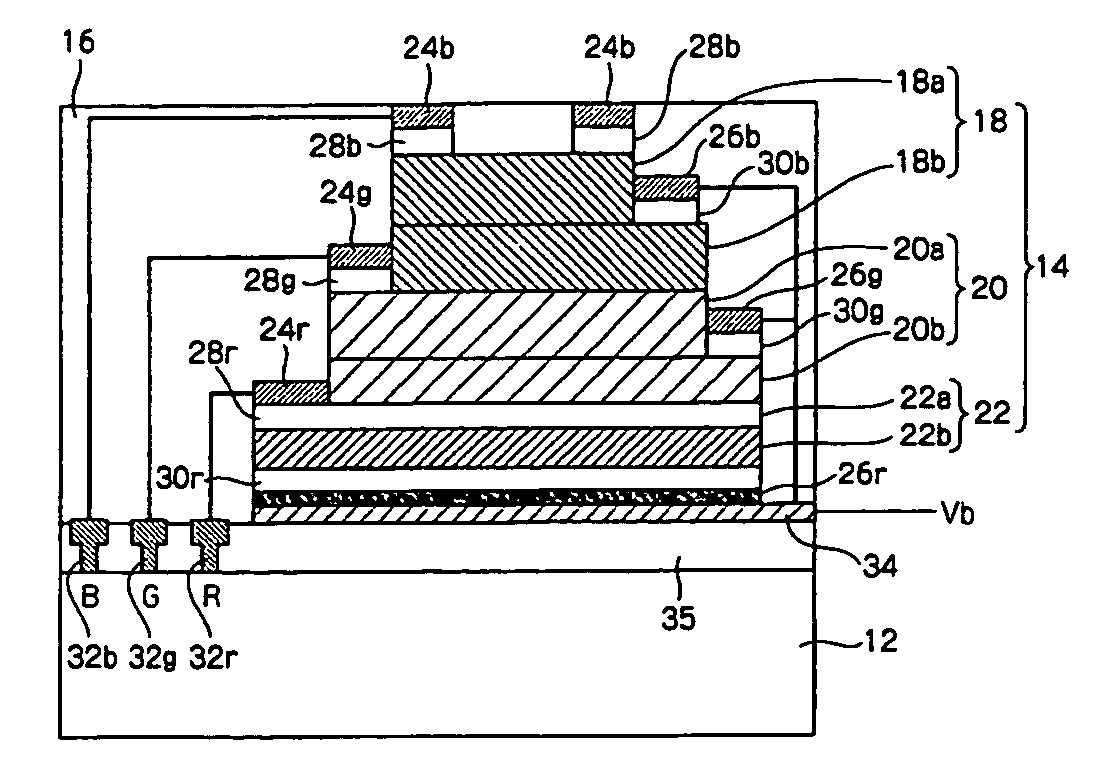
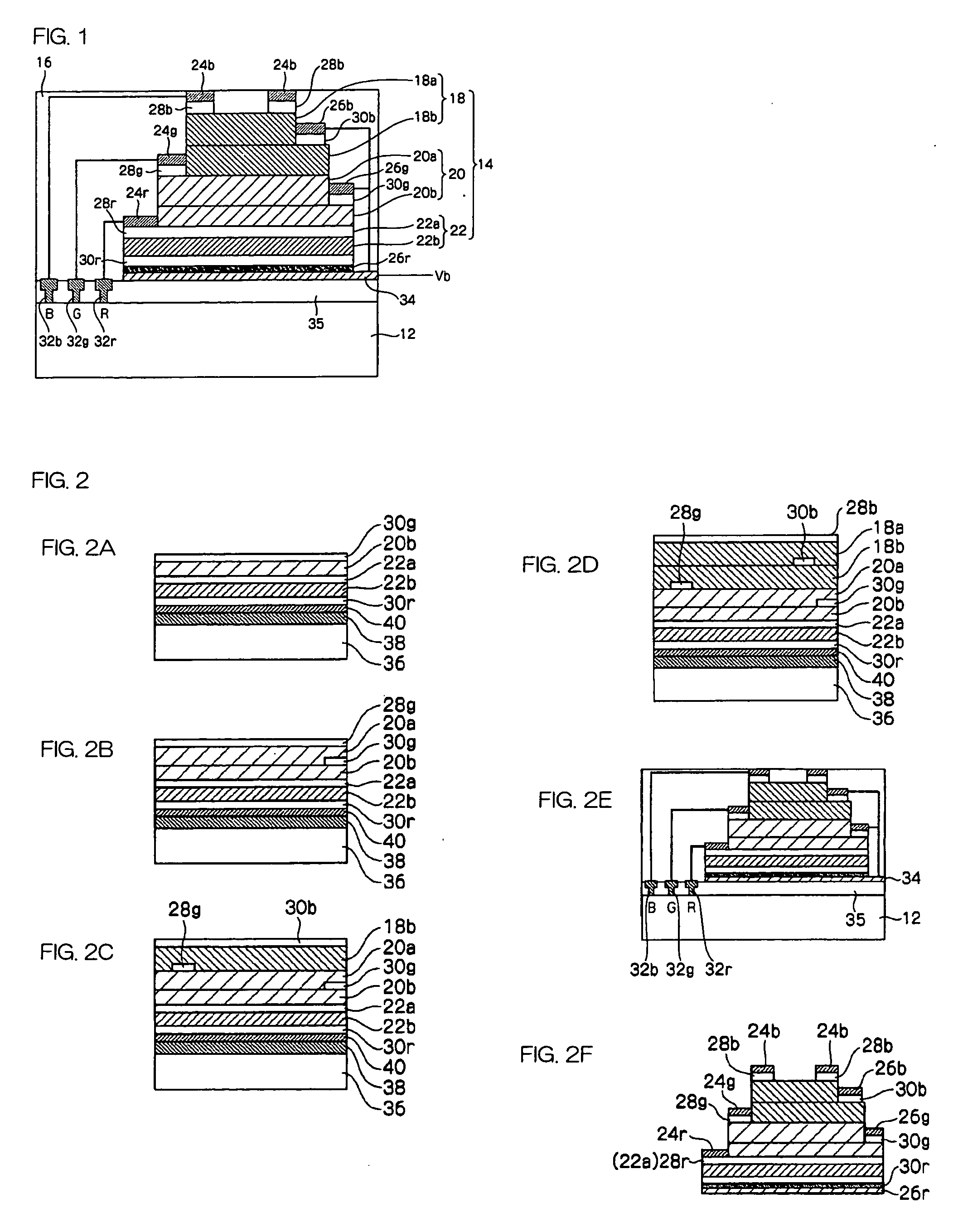
[0024]FIG. 1 is schematic drawing illustrating the configuration of a first embodiment of the solid-state image pickup device of the present invention. FIGS. 2A-2E are schematic drawings illustrating the production process for the first embodiment of the solid-state image pickup device of the present invention.

[0025] In a solid state image pickup device 10 according to the present embodiment, a photoelectric conversion unit 14 is formed on a signal transmission circuit board 12 (silicon substrate) having a signal transmission circuit (not shown in the figures) formed thereon. The solid state image pickup device 10 is sealed with an insulating sealer 16, except for a light-receiving surface of the photoelectric conversion unit 14. Although not shown in the figures, a transparent insulation film may be formed over the top layer of the photoelectric conversion unit 14 for protection of the light-receiving surface.

[0026] T...

second embodiment

of the Solid-State Image Pickup Device of the Present Invention

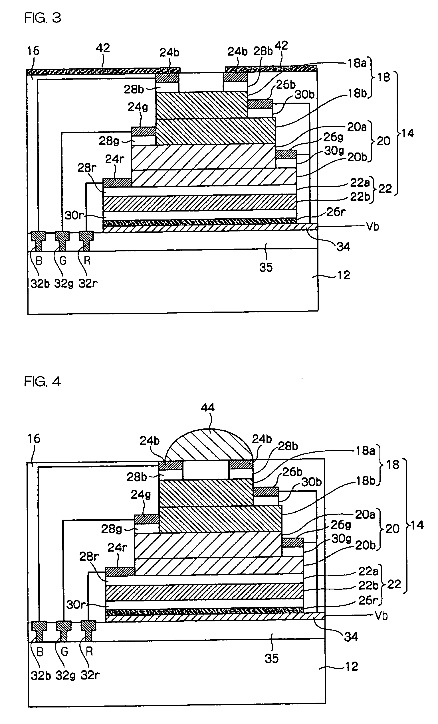
[0050]FIG. 3 is schematic drawing illustrating the configuration of a second embodiment of the solid-state image pickup device of the present invention.

[0051] In the solid state image pickup device 10 of this embodiment, a light-shielding film 42 is formed on a photoelectric conversion unit 14 except on its light-receiving surface. The light-shielding film 42 can be formed, for example, by masking the light-receiving surface and depositing a metal material on the sealer 16 of the photoelectric conversion unit 14. Aside from this, the structure is the same as in the first embodiment, and thus, description thereof is omitted.

[0052] In the solid state image pickup device 10 of this embodiment, by forming a light-shielding film 42 on the photoelectric conversion unit 14 and thus shielding the unit from light except at the light-receiving surface, it becomes possible to effectively prevent color mixing even when the solid s...

third embodiment

of the Solid-State Image Pickup Device of the Present Invention

[0053]FIG. 4 is schematic drawing illustrating the configuration of a third embodiment of the solid-state image pickup device of the present invention.

[0054] In the solid state image pickup device 10 of this embodiment, a microlens 44 is formed on or above the light-receiving surface of the photoelectric conversion unit 14. Aside from this, the structure is the same as in the first embodiment, and thus, description thereof is omitted.

[0055] The solid state image pickup device 10 of this embodiment, which has a microlens 44 formed on or above the light-receiving surface of the photoelectric conversion unit 14, has a higher incident light-converging efficiency, allowing more effective increase in sensitivity and higher color separation.


PUM


Abstract

The present invention provides a solid state image pickup device, including a silicon substrate and a photoelectric conversion unit which receives external incident light and generates signals in accordance therewith, and which is formed on or above the surface of the silicon substrate, wherein a signal transmission circuit for reading out the signals generated in the photoelectric conversion unit is formed on the silicon substrate; the photoelectric conversion unit includes a photoelectric conversion layer which has a laminated structure of plural compound semiconductor layers, which are different from each other in light wavelength to absorb and are provided with the laminated structure so that the shorter a light absorption wavelength of a compound semiconductor layer is, the closer to a light incident side the compound semiconductor layer resides; and the plural compound semiconductor layers are respectively connected to pixel electrodes formed on the signal transmission circuit.

Description

CROSS-REFERENCE TO RELATED APPLICATION [0001] This application claims priority under 35 USC 119 from Japanese Patent Application No. 2004-244081, the disclosure of which is incorporated by reference herein. BACKGROUND OF THE INVENTION [0002] 1. Field of the Invention [0003] The present invention relates to a solid-state image pickup device which is applicable to any other apparatuses including digital cameras, video cameras, facsimile machines, scanners, copying machines and the like, and any other optical sensors including bio-sensors, chemical sensors and the like. Particularly, the present invention relates to a solid-state image pickup device which has a laminated type photoelectric conversion layer. [0004] 2. Description of the Related Art [0005] Solid state image pickup devices having a structure in which a photoelectric conversion layer is provided on the plane almost identical with that of a charge transfer path have had disadvantages accompanying higher integration of pixel...

Claims


Application Information

Patent Timeline
IPC IPC(8): H02N6/00H01L27/146H01L31/10H04N5/335H04N5/357H04N5/369
CPCH01L27/14623H01L31/101H01L31/02164H01L27/14647
Inventor FUKUNAGA, TOSHIAKIYOKOYAMA, DAISUKE
Owner FUJIFILM HLDG CORP
Why Eureka
Try Eureka