Method of bonding and bonding apparatus for a semiconductor chip

Inactive Publication Date: 2006-03-02
FUJITSU LTD
View PDF9 Cites 9 Cited by
  • Summary
  • Abstract
  • Description
  • Claims
  • Application Information

AI Technical Summary

Benefits of technology

[0038] With the method of bonding and bonding apparatus for a semiconductor chip according to Claims 1 to 4 and 6 to 9, the half-wavelength of the compressional waves of the ultrasonic vibration is set at a length given by multiplying a gap between adjacent electrode terminals by a reciprocal of a natural number, and maximum amplitude points of the compressional waves are located at positions of the respective electrode terminals, so that it is possible to bond the electrode terminals using extremely high frequency ultrasonic vibration and the bonding strength of bonds between the electrode terminals can be incre

Problems solved by technology

However, in the conventional method of bonding a semiconductor chip that uses ultrasonic vibration, there is the problem that when the bonding characteristics o

Method used


Image

  • Method of bonding and bonding apparatus for a semiconductor chip
  • Method of bonding and bonding apparatus for a semiconductor chip
  • Method of bonding and bonding apparatus for a semiconductor chip

Examples


first embodiment

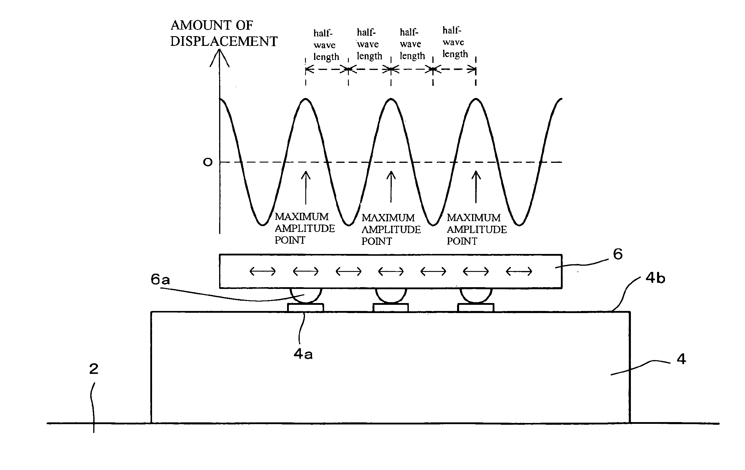
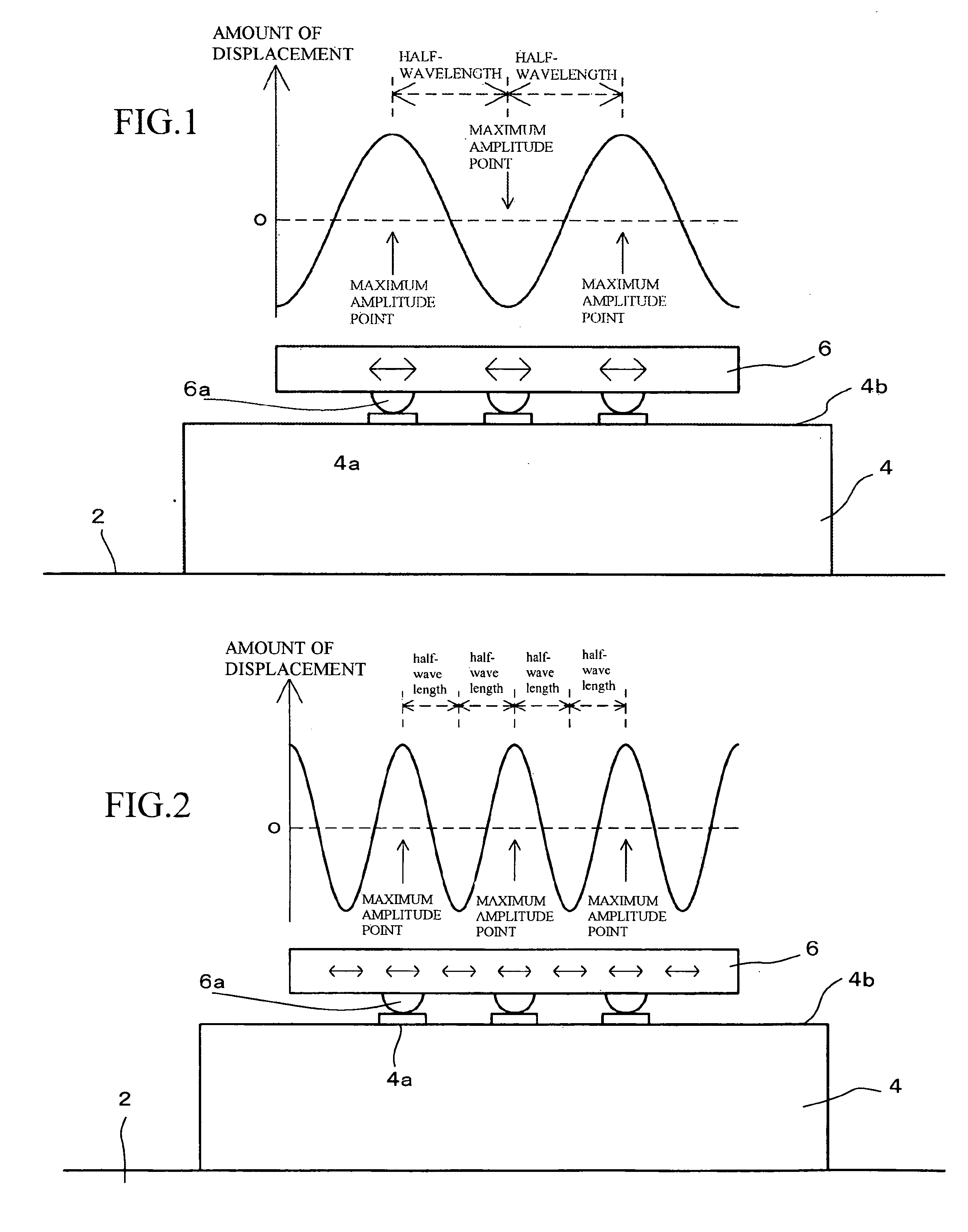
[0060] Specific examples of a method and an apparatus that apply ultrasonic vibration set as described above to the semiconductor chip 6 are shown in FIG. 3.

[0061] As shown in FIG. 3, the ends of an ultrasonic vibrator 10 are attached to horns 12 as a contact body and end parts of the horn 12 are placed in contact with side surfaces of the semiconductor chip 6. By having the ultrasonic vibrator 10 ultrasonically vibrate using a vibration control apparatus (not shown), ultrasonic bonding can be applied to the semiconductor chip 6 via the horn 12.

[0062] The horn 12 is formed so as to be tapered from the ultrasonic vibrator 10 side toward the tip, so that the ultrasonic vibration can be amplified toward the tip of the horn 12 and ultrasonic vibration with a large amplitude can be effectively transmitted to the semiconductor chip 6.

[0063] It should be noted that the contact body does not need to be a horn. Also, the ultrasonic vibrator 10 may be placed in direct contact with the semi...

second embodiment

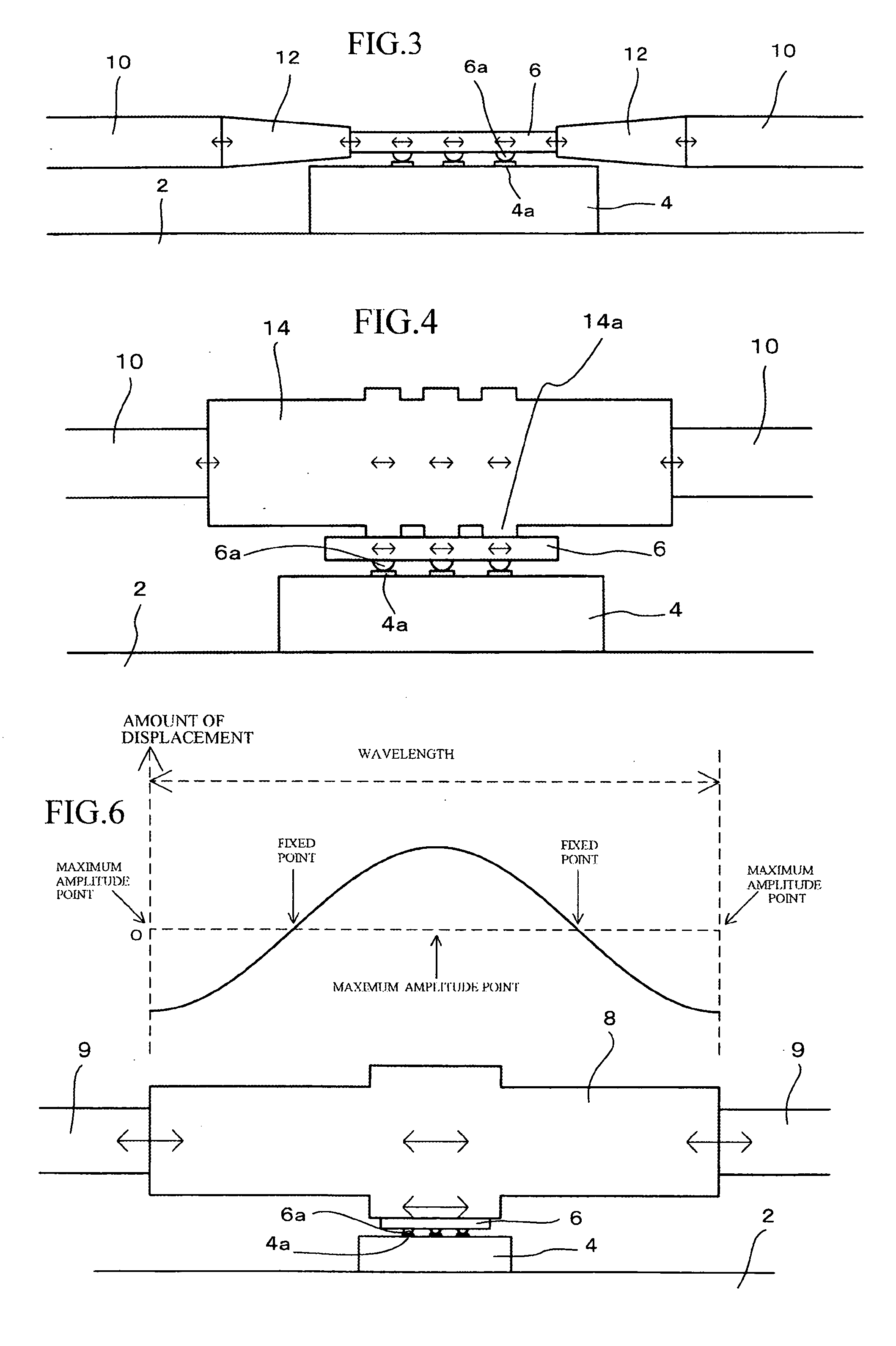
[0065] Next, other examples of the method and apparatus for applying ultrasonic vibration to the semiconductor chip 6 will be described with reference to FIG. 4.

[0066] In FIG. 4, the circuit board 4 is held on a stage 2. The semiconductor chip 6 is held on a bonding tool 14 (mount head) as a contact body and is moved together with the bonding tool 14, and is positioned so that the bumps 6a, 6a, . . . provided on the semiconductor chip 6 are respectively placed in contact with the corresponding pads 4a, 4a, . . . provided on the circuit board 4.

[0067] Both end surfaces of the bonding tool 14 are connected to the ultrasonic vibrator 10, and by having the ultrasonic vibrator 10 ultrasonically vibrate in a horizontal direction using a vibration control apparatus (not shown), the bonding tool 14 and the semiconductor chip 6 are ultrasonically vibrated together.

[0068] On the bonding tool 14, protruding parts 14a are formed at positions corresponding to the respective electrode terminal...

third embodiment

[0070] While the first and second embodiments are constructions that apply compressional waves to the semiconductor chip 6, a third embodiment relates to Claims 5 and 10 of this application and is a construction that vibrates the entire semiconductor chip 6 at high frequency.

[0071]FIGS. 5A and 5B are diagrams useful in explaining the construction of the third embodiment.

[0072] It should be noted that since the bonding apparatus for a semiconductor chip according to the third embodiment has the same fundamental construction as the second embodiment, description is omitted for parts of the construction that are common to the second embodiment and only different parts of the construction are described.

[0073] Protruding parts 16a that contact the semiconductor chip 6 are provided on the bonding tool 16 at fixed gaps. However, unlike the protruding parts 14a of the second embodiment, the formation positions of the protruding parts 16a do not need to be located at positions correspondi...


PUM

PropertyMeasurementUnit
Lengthaaaaaaaaaa
Wavelengthaaaaaaaaaa

Abstract

A method of bonding and a bonding apparatus for a semiconductor chip uses ultrasonic vibration but can improve the bonds between electrode terminals of a semiconductor chip and a substrate. In a method of bonding a semiconductor chip that places electrode terminals of the semiconductor chip and electrode terminals of a substrate in contact and applies ultrasonic vibration to the semiconductor chip to bond the electrode terminals of the semiconductor chip and the substrate together, the ultrasonic vibration is compressional waves that are transmitted to the semiconductor chip and is set so that a half-wavelength of the ultrasonic vibration is a length given by multiplying a gap between adjacent electrode terminals in a direction of the compressional waves by a reciprocal of a natural number, and maximum amplitude points are located at positions of the respective electrode terminals of the semiconductor chip and the substrate.

Description

BACKGROUND OF THE INVENTION [0001] 1. Field of the Invention [0002] The present invention is a method of bonding and bonding apparatus for a semiconductor chip that places electrode terminals of a semiconductor chip and electrode terminals of a substrate in contact and applies ultrasonic vibration to the semiconductor chip to bond the electrode terminals of the semiconductor chip and the substrate together. [0003] 2. Related Art [0004] In recent years, when flip-chip bonding a semiconductor chip to a circuit board during the manufacturing of a semiconductor device such as a semiconductor package, a method is used where electrode terminals such as bumps of the semiconductor chip are placed in contact with electrode terminals such as pads of the circuit board and ultrasonic vibration is applied to the semiconductor chip to bond the electrode terminals of the semiconductor chip and the printed circuit board together. [0005] A conventional method of flip-chip bonding that uses ultrasoni...

Claims


Application Information

Patent Timeline
IPC IPC(8): B23K1/06
CPCB23K20/10H01L2924/01033H01L24/75H01L24/81H01L2224/16H01L2224/75H01L2224/75305H01L2224/81205H01L2224/81801H01L2924/01013H01L2924/01079H01L2924/01005H01L2924/01006H01L2924/01023B23K2201/40B23K2101/40
Inventor MATSUMURA, TAKAYOSHI
Owner FUJITSU LTD
Why Eureka
Try Eureka