Method to selectively recess ETCH regions on a wafer surface using capoly as a mask

Active Publication Date: 2006-03-02
TEXAS INSTR INC
View PDF6 Cites 25 Cited by
  • Summary
  • Abstract
  • Description
  • Claims
  • Application Information

AI Technical Summary

Benefits of technology

[0009] According to one aspect of the invention, a CAPOLY layer is formed over an NMOS region of a semiconductor device. A recess etch is performed on active regions of devices within a PMOS region of the semiconductor device wherein the CAPOLY layer prevents etching of devices within an NMOS region of the semi

Problems solved by technology

However, the compressive strain that improves hole mobility can degrade electron mobility and the tensile strain that improves electron mobility can also degrade hole mobility.
As a result, introducing tensile strain, such as by using a CAP layer, can impro

Method used


Image

  • Method to selectively recess ETCH regions on a wafer surface using capoly as a mask
  • Method to selectively recess ETCH regions on a wafer surface using capoly as a mask
  • Method to selectively recess ETCH regions on a wafer surface using capoly as a mask

Examples


Embodiment Construction

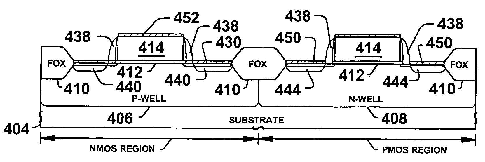
[0015] One or more implementations of the present invention will now be described with reference to the attached drawings, wherein like reference numerals are used to refer to like elements throughout, and wherein the illustrated structures are not necessarily drawn to scale. The invention provides transistor structures and methods in which transistor mobility is improved while reducing masks employed in fabrication thereof.

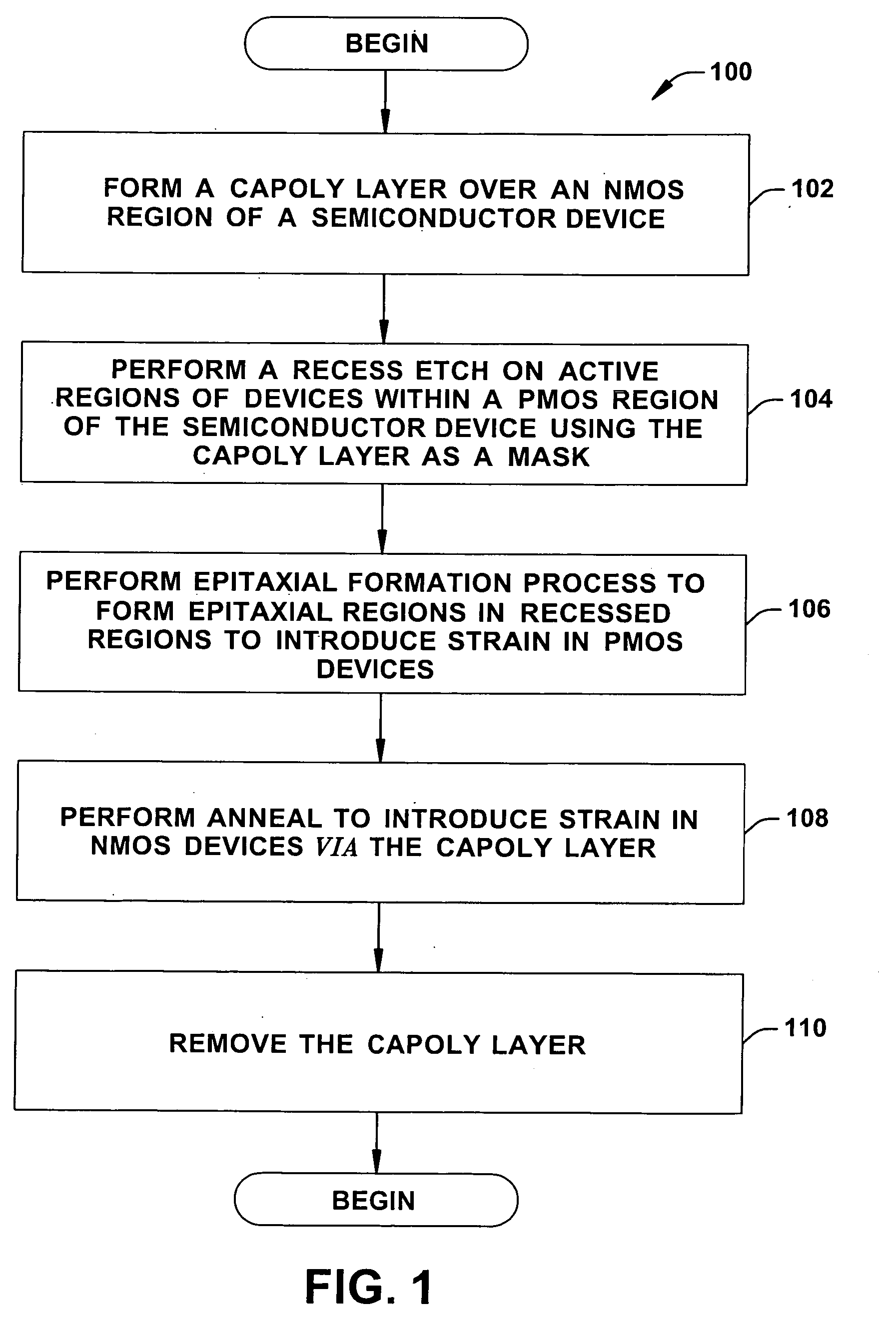
[0016]FIG. 1 is a flow diagram illustrating a method 100 of fabricating a semiconductor device that selectively introduces strain into channel regions of transistor devices located within NMOS and PMOS regions of a semiconductor device in accordance with an aspect of the present invention.

[0017] The method 100 begins at block 102 wherein a CAPOLY layer, also referred to as a stacked poly cap, is formed over an NMOS region of the semiconductor device. The CAPOLY layer is formed by depositing and / or growing one or more layers of materials (e.g., oxide, nitride, a...


PUM


Abstract

The present invention facilitates semiconductor fabrication by providing methods of fabrication that selectively apply strain to channel regions of devices while mitigating masking operations employed. A CAPOLY layer is formed over an NMOS region of a semiconductor device (102). A recess etch is performed on active regions of devices within a PMOS region of the semiconductor device (104) and the CAPOLY layer prevents etching of devices within an NMOS region of the semiconductor device. Subsequently, an epitaxial formation process (106) is performed that forms or deposits epitaxial regions and introduces a first type of strain across the channel regions in the PMOS region. Then, the semiconductor device is annealed (108) to cause the CAPOLY layer to introduce a second type of strain across the channel regions in the NMOS region. After annealing, the CAPOLY layer is removed (110).

Description

FIELD OF INVENTION [0001] The present invention relates generally to semiconductor devices and more particularly to transistors and associated methods of manufacture having improved mobility due to channel strain. BACKGROUND OF THE INVENTION [0002] A conventional MOS transistor generally includes a semiconductor substrate, such as silicon, having a source, a drain, and a channel positioned between the source and drain. A gate stack composed of a conductive material (a gate conductor), an oxide layer (a gate oxide), and sidewall spacers, is typically located above the channel. The gate oxide is typically located directly above the channel, while the gate conductor, generally comprised of polycrystalline silicon (polysilicon) material, is located above the gate oxide. The sidewall spacers protect the sidewalls of the gate conductor. [0003] Generally, for a given electric field across the channel of a MOS transistor, the amount of current that flows through the channel is directly prop...

Claims


Application Information

Patent Timeline
IPC IPC(8): H01L21/8238
CPCH01L21/823807H01L21/823814H01L29/7848H01L29/7843H01L29/7842
Inventor ROTONDARO, ANTONIO L.P.SRIDHAR, SEETHARAMAN
Owner TEXAS INSTR INC
Why Eureka
Try Eureka