Method for manufacturing soi wafer and soi wafer

a manufacturing method and technology for soi wafers, applied in semiconductor/solid-state device manufacturing, basic electric elements, electric apparatus, etc., can solve the problems of difficult to obtain a good crystal low quality of buried oxide layer, and inability to form thin layers of buried oxide film, etc., to achieve easy production, crystallinity and surface quality of soi layer are excellent, and the crystallinity and surface quality is excellen

Inactive Publication Date: 2006-03-09
SHIN-ETSU HANDOTAI CO LTD
View PDF14 Cites 32 Cited by
  • Summary
  • Abstract
  • Description
  • Claims
  • Application Information

AI Technical Summary

Benefits of technology

[0015] Accordingly, the present invention was conceived in view of the above problems. An object of the present invention is to provide a method of producing an SOI wafer in which by using SIMOX method, there can be produced a high quality SOI wafer having a buried oxide film of which the film thickness is thin and perfectness is high, and an SOI layer of which crystallinity and surface quality are extremely good.

Problems solved by technology

However, in the case of performing the oxygen ion implantation by the high dose amount as above by using SIMOX method, although perfectness of the buried oxide film can be enhanced, there is an problem that it is difficult to obtain an SOI layer having a good crystal quality because damage is introduced to the wafer surface transmitted by a large amount of the oxygen ions so that threading dislocation is easily generated at high density in the SOI layer when performing the oxide film-forming heat treatment.
However, when an SOI wafer is produced by using SIMOX method as above, for example if oxygen ions are implanted by high dose amount required to form the continuous buried oxide film, a thickness of a buried oxide film formed an SOI wafer always become thicker than one thickness, and it was impossible to form the buried oxide film with a thin thickness as described above.
However, because a quality of the buried oxide film is low, it is necessary to perform ITOX treatment to improve the quality of the buried oxide film as described above, and the buried oxide film in the silicon wafer is thickened to be thick one.
Accordingly, it was extremely difficult to produce, by SIMOX method, an SOI wafer having the buried oxide film of which perfectness is high and the film thickness is thin as required in these days.
However, there are problems that crystal defects existing in the SOI layer are much and crystallinity of the SOI layer is inferior and also surface roughness of the SOI layer is large.

Method used


Image

  • Method for manufacturing soi wafer and soi wafer
  • Method for manufacturing soi wafer and soi wafer
  • Method for manufacturing soi wafer and soi wafer

Examples


example 1

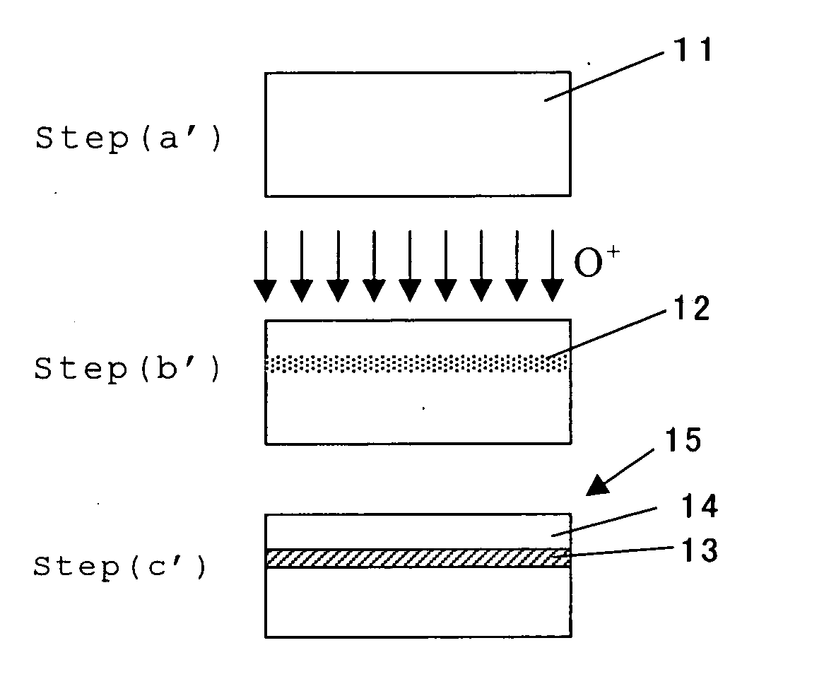
[0065] Mirror-polished silicon wafers having a diameter of 200 mm were prepared to produce SOI wafers having a buried oxide film with a thickness of 80 nm as product specifications by SIMOX method.

[0066] First, an oxygen ion-implanted layer was formed in the silicon wafer by implanting oxygen ions into the silicon wafer heated at a temperature of about 500° C. from one main surface thereof under a condition that implantation energy is set 180 keV and dose amount is set 4.0×10¹⁷ / cm2. Sequentially, after buried oxide film-forming heat treatment is performed in an argon gas atmosphere in which an oxygen concentration is 0.5% at 1350° C. for 4 hours to convert the oxygen ion-implanted layer to a buried oxide film, the buried oxide film in the silicon wafer was thickened by performing ITOX treatment in a mixed gas atmosphere of an argon gas and an oxygen gas (oxygen concentration is 70%) at 1350° C. for 4 hours.

[0067] Next, after the oxide film formed on the wafer surface was etched to...

example 2

[0073] Several SOI wafers made under the same condition as above Example 1 and having buried oxide film with a thickness of 80 nm were prepared. Heat treatment to reduce the thickness of the buried oxide film which was performed in an argon gas atmosphere (Oxide concentration was 10 ppm or less) at 1200° C. was added to them by adjusting heat treatment time. Thereby there could be obtained SOI wafers of which final buried oxide film thickness were 40 nm, 20 nm, 10 nm, and 5 nm. And, as to the SOI wafers, as a result of measurement of density of HF defects and density of pin holes similarly as Example 1, they were observed to be equal to those of Example 1 and Comparative example 1.

[0074] As described above, according to the present invention, even if SIMOX method by which an SOI wafer can be produced from one wafer is adopted without using bonding method which requires two wafers when producing an SOI wafer, there can be obtained a high quality SOI wafer of which buried oxide film ...


PUM


Abstract

The present invention provides a method of producing an SOI wafer, comprising at least steps of forming an oxygen ion-implanted layer by implanting oxygen ions into a silicon wafer from one main surface thereof, subjecting the silicon wafer to oxide film-forming heat treatment to convert the oxygen ion-implanted layer into a buried oxide film, and thereby producing an SOI wafer having an SOI layer on the buried oxide film, wherein when the buried oxide film is formed in the silicon wafer, the buried oxide film is formed so that a thickness thereof is thicker than a thickness of the buried oxide film which the SOI wafer to be produced has, and thereafter the silicon wafer in which the thicker buried oxide film is formed is subjected to a heat treatment to reduce the thickness of the buried oxide film. Thereby, there can be provided a method of producing an SOI wafer in which a high quality SOI wafer having a buried oxide film of which a film thickness is thin and perfectness is high and an SOI layer of which crystallinity and surface quality are extremely good can be produced by using SIMOX method.

Description

TECHNICAL FIELD [0001] The present invention relates to a method of producing an SOI (Silicon on insulator) wafer having SOI structure in which a silicon layer is formed on an insulator, and an SOI wafer produced by the method thereof. BACKGROUND ART [0002] Recently, an SOI wafer having SOI structure in which a silicon layer (an SOI layer) is formed on an insulator has been especially attracting attention as a wafer for high-performance LSI for an electronic device because the SOI wafer is excellent in high-speed property, low power consumption, high breakdown voltage, environmental resistance, etc. of the device. [0003] Representative production methods of the SOI wafer are bonding method, SIMOX (Separation by ion-implanted oxygen) method, and so on. The bonding method is a method of producing an SOI wafer by forming an oxide film on at least one of a bond wafer to form an SOI layer and a base wafer to be a supporting substrate, bonding the bond wafer to the base wafer through the ...

Claims


Application Information

Patent Timeline
Patent Type & Authority Applications(United States)
IPC IPC(8): H01L21/425H01L21/22H01L21/265H01L21/762
CPCH01L21/76243H01L21/26533H01L21/02H01L21/20
Inventor YOKOKAWA, ISAOAGA, HIROJITAKANO, KIYOTAKAMITANI, KIYOSHI
Owner SHIN-ETSU HANDOTAI CO LTD
Why Eureka
Try Eureka