Organic semiconductor device

a semiconductor and organic technology, applied in the direction of solid-state devices, transistors, thermoelectric devices, etc., can solve the problem that the charge is not easily injected achieve the effect of easy charge carrier injection high speed, and effective and rapid supply to the organic semiconductor layer

Inactive Publication Date: 2006-03-16
DAI NIPPON PRINTING CO LTD
View PDF1 Cites 45 Cited by
  • Summary
  • Abstract
  • Description
  • Claims
  • Application Information

AI Technical Summary

Benefits of technology

[0007] On the other hand, in a field of an organic electroluminescence (hereinafter, referred to as organic EL), as described in Japanese Patent Application Laid-open (JP-A) No. 2002-270369, an organic EL element is reported in which an organic thin film having dipole moment having electric double layer effect is formed, as a hole injection promoting layer, on a light emitting layer side surface of an anode. This report describes an accomplishment of lowering operating voltage by making the energy gap between the electrode and the light emitting layer, by a function of the organic thin film having dipole moment, so that the hole injection from the anode to the light emitting layer is made easy. Moreover, as described in Tokuhyou No. 2001-5122145, the organic EL element is reported in which the organic thin film comprising a dipole compound having functional group such as π-electron system, is formed, as the hole injection promoting layer, on the light emitting layer side surface of the anode. In this report, it is described that the charge injection from the electrode to the light emitting layer is made easy because the organic thin film acts as the electric double layer which makes the energy gap between the electrode and the light emitting layer smaller.
[0028] According to the organic semiconductor device of the present invention, since the charge carrier injection promoting layer is provided in between the organic semiconductor layer and at least one electrode of the first electrode and the second electrode facing to each other, the charge carrier injection to the organic semiconductor layer is made easy. As a result, the charge carrier, which is sufficient in quantity for carrier mobility, is supplied to the organic semiconductor layer effectively and swiftly. Particularly, since sufficient quantity of charge is supplied to the organic semiconductor layer formed from the liquid crystalline organic semiconductor material, the organic semiconductor device having such organic semiconductor layer can transfer a lot of charge at high speed.

Problems solved by technology

However, since there is a large energy gap between the organic semiconductor layer and the source electrode supplying the charge, there is a problem that the charge is not injected to the organic semiconductor layer easily.

Method used


Image

  • Organic semiconductor device
  • Organic semiconductor device
  • Organic semiconductor device

Examples


example 1

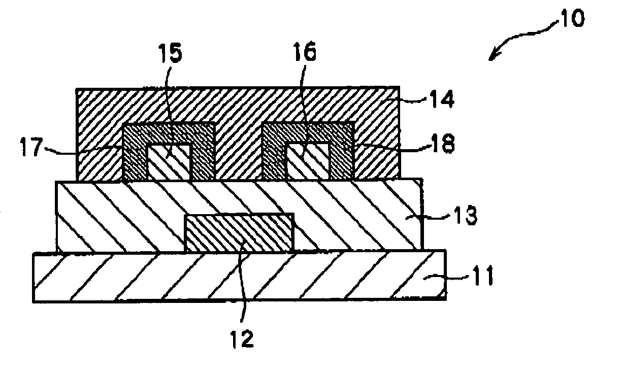
[0108] As the organic semiconductor device in Example 1, a staggered type organic transistor element was prepared.

[0109] On a non-alkali glass substrate, (manufactured by Corning Incorporated, product number: 1737), an ITO thin film of 10 Ωcm sheet resistance was formed by sputtering method, and a pair of drains source electrode of 50 μm channel length and 1 mm channel width was formed by photolithography method. In order to inhibit non-desirable leak current deriving from conduction path, a passivation film comprising SiO2 sputtering film was provided on the glass substrate, provided with the pair of drain•source electrode, by the photolithography method and lift off method so that only the organic transistor element forming region is bared.

[0110] Prier to the formation of the charge carrier injection promoting layer, the glass substrate provided with the source electrode and the drain electrode was subjected to ultrasonic cleaning with aceton, alkali detergent (manufactured by F...

example 2

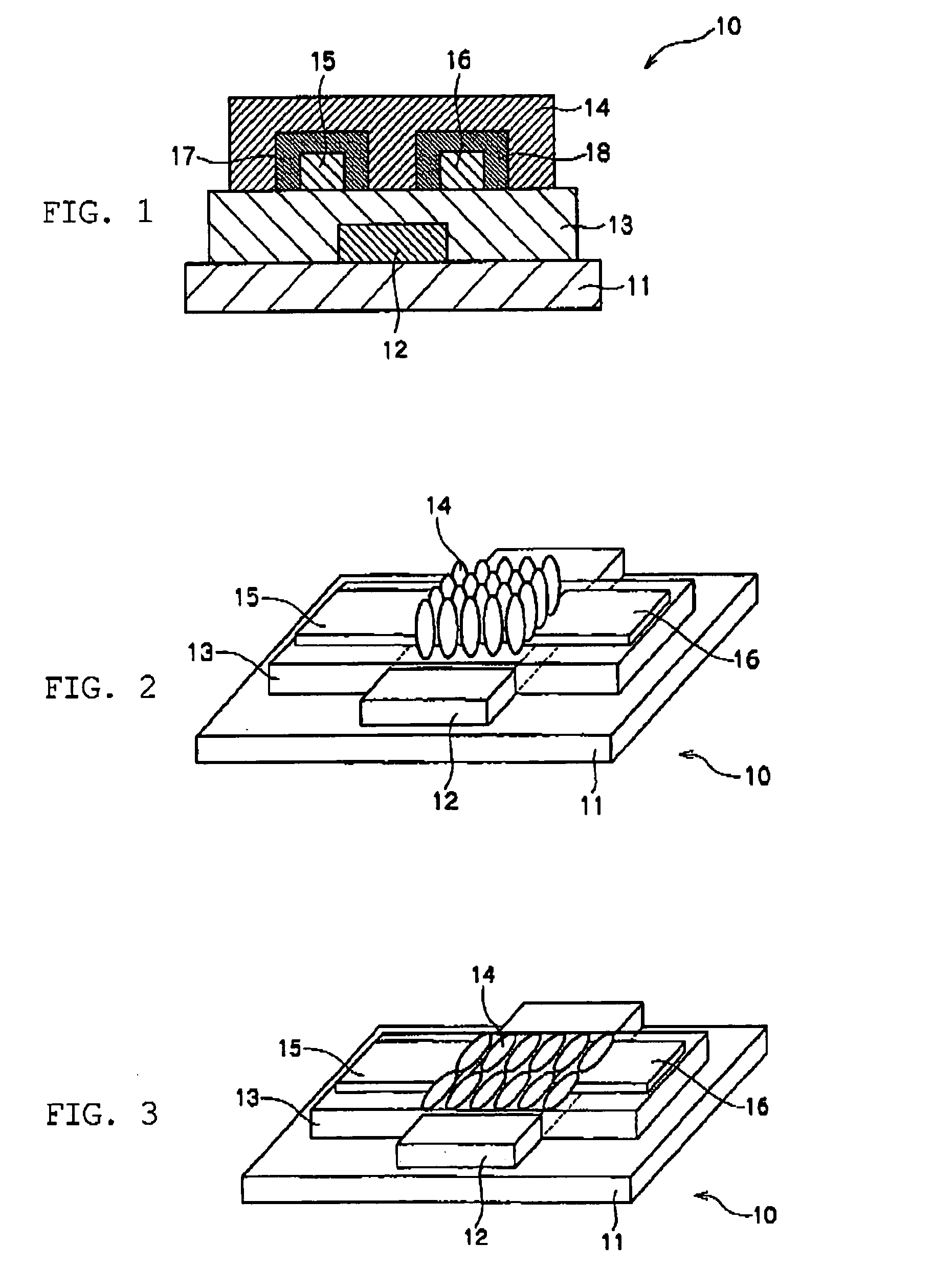
[0116] As the organic semiconductor device in Example 2, an organic transistor element of coplanar type electrode configuration was prepared.

[0117] First, on a high-doped π-type silicone substrate, 300 nm of SiO2 layer was formed by heat oxidation, and a gate electrode substrate provided with a gate-insulating layer was obtained. This gate electrode substrate serves as both a gate electrode and a substrate. Next, on the gate-insulating layer formed surface of the substrate, an ITO thin film of 10 Ωcm sheet resistance was formed by sputtering me-hod, and a pair of drain•source electrode of 50 μm channel length and 1 mm channel width was formed by photolithography method. A passivation film was provided on the glass substrate, provided with the pair of drain•source electrode, by the same way as Example 1.

[0118] After cleaning the gate electrode substrate, provided with the source electrode and the drain electrode, by the same way as Example 1, a charge carrier injection promoting la...

example 3

[0120] As the organic semiconductor device in Example 3, an organic transistor element, in which the charge is transported in a direction of a thickness of the organic semiconductor layer, was prepared.

[0121] First, by the same way as Example 2, a gate electrode substrate provided with a gate-insulating layer was obtained. Next, on the gate-insulating layer formed surface of the substrate, an ITO thin film of 10 Ωcm sheet resistance was formed by sputtering method to form a source electrode. A passivation film was provided on the glass substrate provided with the source electrode, by the same way as Example 1.

[0122] After cleaning the gate electrode substrate provided with the source electrode, by the same way as Example 1, a charge carrier injection promoting layer of ClBP, mainly a monolayer, for making the hole injection to the drain•source electrodes formed side surface of the gate electrode substrate easier, was formed by the same way as Example 1. Further, by the same way as...


PUM


Abstract

The present invention provides an organic semiconductor device comprising an organic semiconductor layer having good charge carrier transport property, wherein a carrier injection to the organic semiconductor layer is easy. The above problem is solved by an organic semiconductor device comprising a first electrode and a second electrode facing to each other, and an organic semiconductor layer provided in between the first electrode and the second electrode, wherein a charge carrier injection promoting layer is formed in between the organic semiconductor layer and at least one electrode of the first electrode and the second electrode.

Description

BACKGROUND OF THE INVENTION [0001] 1. Field of the Invention [0002] The present invention relates to an organic semiconductor device. Particularly, the present invention relates to an organic semiconductor device comprising an organic semiconductor layer containing a liquid crystalline organic semiconductor material having excellent charge carrier mobility. [0003] 2. Description of the Related Art [0004]FIG. 8 is a sectional view showing one example of a conventional organic semiconductor device. A conventional organic semiconductor device 100 comprises a substrate 101, a gate electrode 102, a gate-insulating layer 103, an organic semiconductor layer 104, a source electrode 105 and a drain electrode 106. In the organic semiconductor device having such configuration, the organic semiconductor layer is required to have sufficient charge carrier mobility. Therefore, the organic semiconductor material having high charge carrier mobility is being investigated recently. [0005] As a materi...

Claims


Application Information

Patent Timeline
Patent Type & Authority Applications(United States)
IPC IPC(8): H01L29/08H01L29/786H01L51/05H01L51/00H01L51/10
CPCH01L51/0052H01L51/0065H01L51/0067H01L51/0068H01L51/105H01L51/0076H01L51/0541H01L51/0545H01L51/0558H01L51/0071H10K85/615H10K85/653H10K85/654H10K85/655H10K85/657H10K85/731H10K10/466H10K10/464H10K10/484H10K10/84
Inventor HANNA, JUNICHIMAEDA, HIROKINAKASA, AKIHIKONAKAGAWA, HIDEHIRO
Owner DAI NIPPON PRINTING CO LTD
Why Eureka
Try Eureka