

Chip-type electronic component and chip resistor
a technology of electronic components and resistors, applied in the manufacture of resistors, resistor details, resistive material coatings, etc., can solve the problems of difficult to recognize the application state of conductive paste, difficult to check the application state of conductive paste, difficult to check the appearance, etc., to achieve the effect of improving the mass production feasibility and speed
- Summary
- Abstract
- Description
- Claims
- Application Information
AI Technical Summary
Benefits of technology
Problems solved by technology
Method used
Image

Examples
example 1
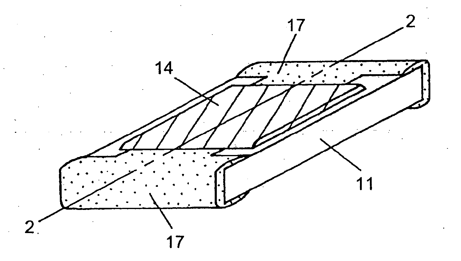
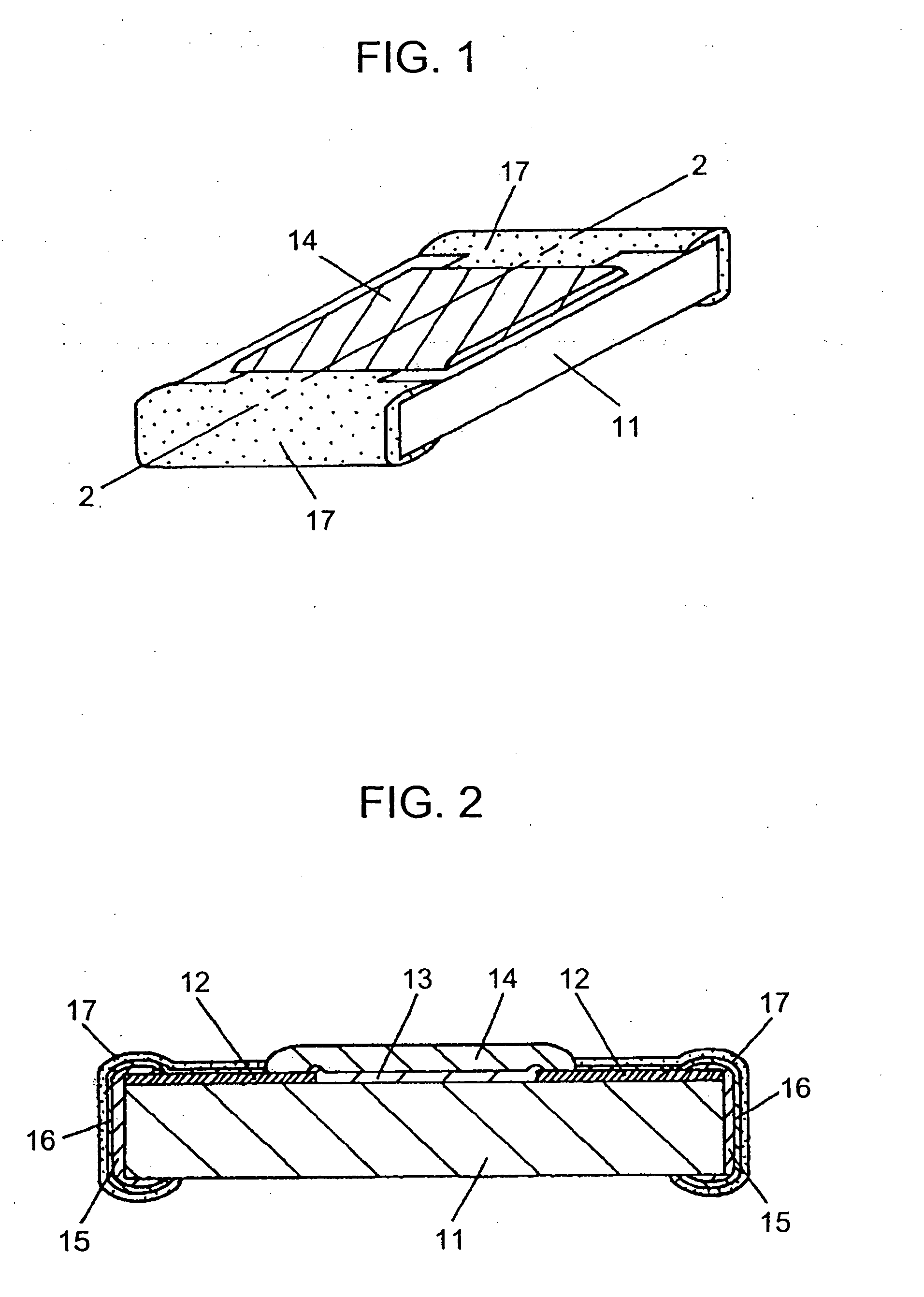
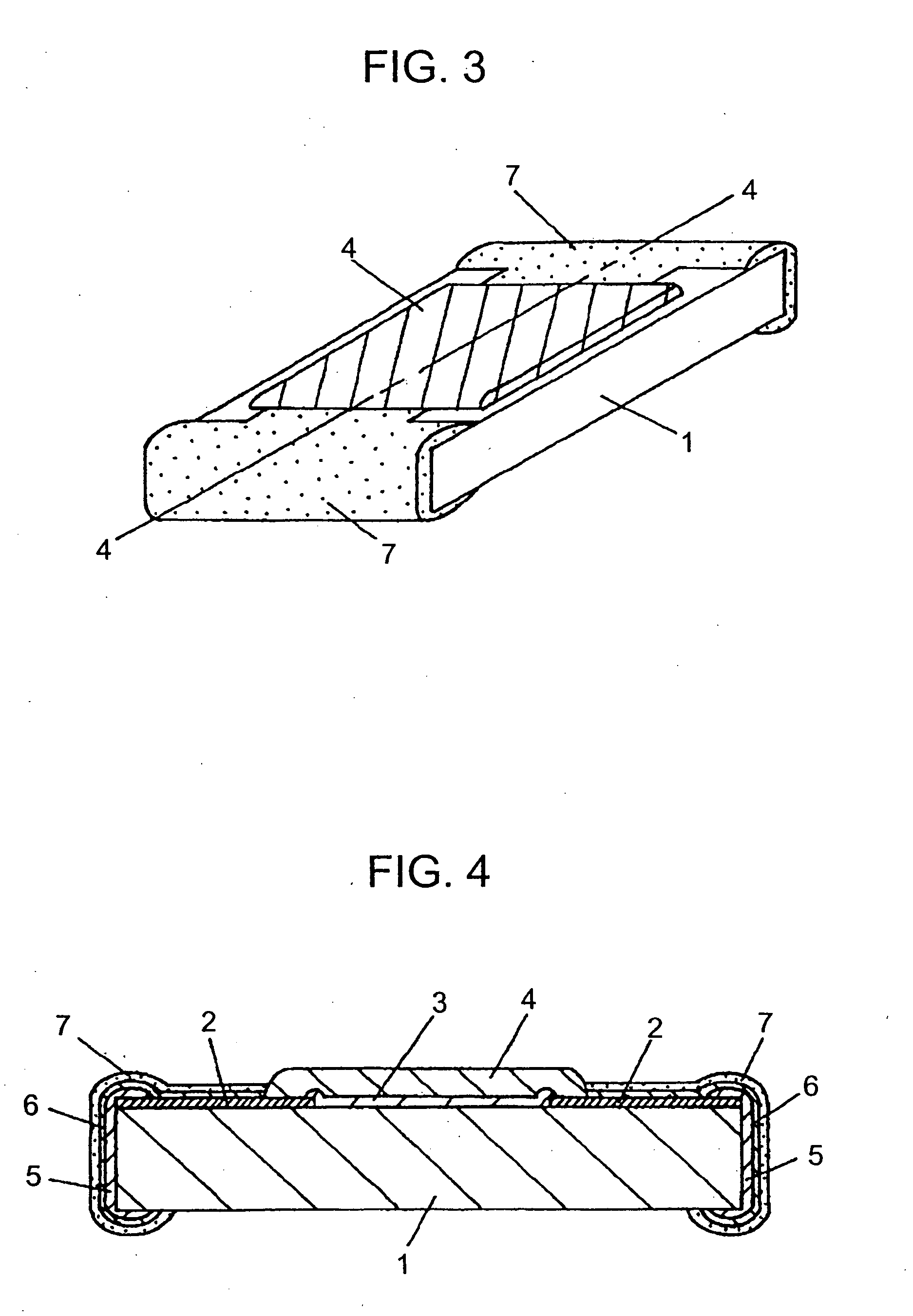
[0040] A structure of a chip resistor in Example 1 of the present invention has the same structure as these of the chip resistor shown in FIG. 1 and FIG. 2. As a resin for the conductive paste for forming side electrodes, bisphenol-A type epoxy resin, a thermosetting resin, and imidazole hardener are used. And spherical silver powder of 0.06 μm in average particle diameter is mixed with the resin at an amount of 85% as spherical conductive particles, and furnace black is further mixed at an amount of 2% as carbon powder.
example 2
[0041] A structure of the chip resistor in Example 2 of the present invention has the same structure as the chip resistor in one embodiment of the present invention shown in FIG. 1 and FIG. 2. As the resin for conductive paste for forming side electrodes, bisphenol-F type epoxy resin, a thermosetting resin, and amine hardener are used. And spherical nickel powder of 2.5 μm in average particle diameter is mixed with the resin at an amount of 90% as spherical conductive particles, and furnace black is further mixed at an amount of 1% as carbon powder.
example 3
[0042] A structure of the chip resistor in Example 3 of the present invention has the same structure as the chip resistor in one embodiment of the present invention shown in FIG. 1 and FIG. 2. As the resin for conductive paste for forming side electrodes, bisphenol-A type epoxy resin, a thermosetting resin, and imidazole hardener are used. And spherical tungsten powder of 10 μm in average particle diameter is mixed with the resin at an amount of 80% as spherical conductive particles, and furnace black is further mixed at an amount of 3% as carbon powder.
PUM
 Abstract
Description
Claims
Application Information