Method of forming a wafer backside interconnecting wire

a backside and interconnecting wire technology, applied in the direction of electrical equipment, semiconductor devices, semiconductor/solid-state device details, etc., can solve the problems of fp bga package suffering from the stress problem between the die and the substrate, the substrate warpage, and the aforementioned technologies still have some disadvantages or limitations, so as to achieve the effect of reducing the area of the package and low cos

Active Publication Date: 2006-03-16
TESSERA ADVANCED TECH
View PDF4 Cites 32 Cited by
  • Summary
  • Abstract
  • Description
  • Claims
  • Application Information

AI Technical Summary

Benefits of technology

[0011] The method according to the present invention is characterized by forming the interconnecting wires on the backside of the wafer, and thus the area of the package is effectively reduced. In addition, since the wafer is diced subsequent to packaging, the method benefits from mass production, low cost and consistency with standard semiconductor processes.

Problems solved by technology

However, this leads to some problems such as the warpage of the substrate 12.
However, the CSP formed by any of the aforementioned technologies still has some disadvantages or limitations.
Regarding the FP BGA technology, although an FP BGA package is consistent with the CSP definition, the FP BGA package suffers from the stress problem between the die and the substrate.
In addition, the gap of two adjacent solder balls is limited, and an excessively small gap causes problems while welding the substrate and the PCB.
Furthermore, if the die and the substrate are packaged by wire bonding, the area of the package cannot be further reduced.
Regarding the FC technology, although the area of an FC package is smaller, the FC technologies cannot be applied to forming some devices, such as optical sensor devices, and print head devices.

Method used


Image

  • Method of forming a wafer backside interconnecting wire
  • Method of forming a wafer backside interconnecting wire
  • Method of forming a wafer backside interconnecting wire

Examples


Embodiment Construction

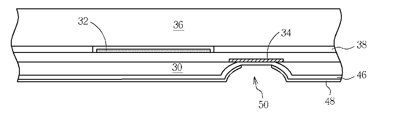
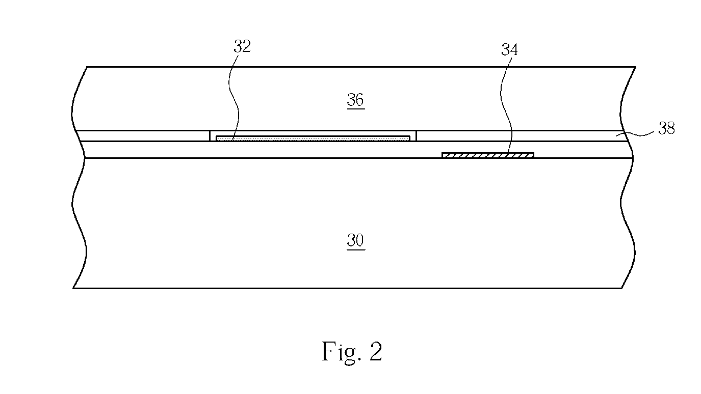
[0015] Please refer to FIG. 2 through FIG. 9. FIG. 2 through FIG. 9 are schematic diagrams illustrating a method of forming a wafer backside interconnecting wire according to a preferred embodiment of the present invention. As shown in FIG. 2, a wafer 30 is provided. The wafer 30 includes at least a circuit element 32 disposed on the front surface of the wafer 30, and at least a metal bonding pad 34 electrically connected to the circuit element 32 positioned on the front surface of the wafer 30. The front surface of the wafer 30 is bonded to a cap wafer 36 with a bonding layer 38. In this embodiment, the material of the bonding layer 38 is particularly selected from commonly used bonding materials, such as photoresist, epoxy, and UV tape, but is not limited to these materials. The cap wafer 36 and the wafer 30 can also be bonded together in another manners, such as by an anode bonding technique or by a plasma enhanced bonding technique. In addition, if the circuit element 32 is an o...


PUM


Abstract

A method of forming a wafer backside interconnecting wire includes forming a mask layer on the back surface, the mask layer including at least an opening corresponding to the bonding pad, performing a first etching process from the back surface to remove the wafer unprotected by the mask layer to form a recess, removing the mask layer, and forming an interconnecting wire on the back surface.

Description

BACKGROUND OF INVENTION [0001] 1. Field of the Invention [0002] The present invention relates to a method of forming a wafer backside interconnecting wire, and more particularly, to a method of forming a wafer level chip scale package (WLCSP) using the wafer backside interconnecting wire. [0003] 2. Description of the Prior Art [0004] The package technologies of integrated circuits are substantially classified into two types: pin through hole (PTH) and surface mounting technology (SMT). Currently, the ball grid array (BGA) package is the most popular SMT type package. Please refer to FIG. 1, which is a schematic diagram of a BGA package 10. As shown in FIG. 1, the BGA package 10 includes a substrate 12, a die 14 bonded to the surface of the substrate 12 with silver glue 16, and a cap layer 18 which covers the die 14 and the surface of the substrate 12. The die 14 includes a circuit layout (not shown) and a plurality of metal bonding pads 20 electrically connected to the circuit layou...

Claims


Application Information

Patent Timeline
Patent Type & Authority Applications(United States)
IPC IPC(8): H01L21/44H01L23/31H01L23/48H01L23/485
CPCH01L23/3128H01L2224/32225H01L2224/05599H01L2224/48227H01L2224/85399H01L2924/01014H01L2924/01047H01L2924/014H01L2924/05042H01L2924/14H01L2924/15311H01L24/05H01L24/48H01L2924/00014H01L2924/01019H01L2924/01033H01L23/481H01L2224/04042H01L2224/73265H01L2224/45099H01L2924/00H01L2924/181H01L21/76898H01L2924/00012
Inventor SHAO, SHIH-FENGYANG, CHEN-HSIUNGPENG, HSIN-YA
Owner TESSERA ADVANCED TECH
Why Eureka
Try Eureka