Optical semiconductor device, optical communication device, and electronic equipment

Inactive Publication Date: 2006-03-23
SHARP KK
View PDF5 Cites 60 Cited by
  • Summary
  • Abstract
  • Description
  • Claims
  • Application Information

AI Technical Summary

Benefits of technology

[0028] An object of the present invention is to provide an optical semiconductor device which has an appropriate light transmittance at temperatures within an operating temperature range and which exhibits excellent operating c

Problems solved by technology

This raises a problem that a difference between the coefficient of linear expansion of the light-permeable mold resin and the coefficients of linear expansion of the optical semiconductor device, the lead frame and the bonding wire would cause disconnection of the bonding wire and occurrence of cracks in the package and the like in a high operating temperature range, as a consequence of which it becomes difficult to produce an optical semiconductor device of high reliability.
As shown in FIG. 18, the general LED, of which the optical output power has the tendency of decrease with the temperature rise, therefore has a problem that a decrease in the optical output power becomes significant at high temperatures and it is difficult to provide an optical semiconductor device having a constant optical output power at temperatures within the operating temperature range.
When the filler is added, the fluctuation in the optical output power has a tendency that the fluctuation cannot be approximated by a linear equation.
As shown in FIG. 19, the conventional optical semiconductor device that uses the

Method used


Image

  • Optical semiconductor device, optical communication device, and electronic equipment
  • Optical semiconductor device, optical communication device, and electronic equipment
  • Optical semiconductor device, optical communication device, and electronic equipment

Examples


first embodiment

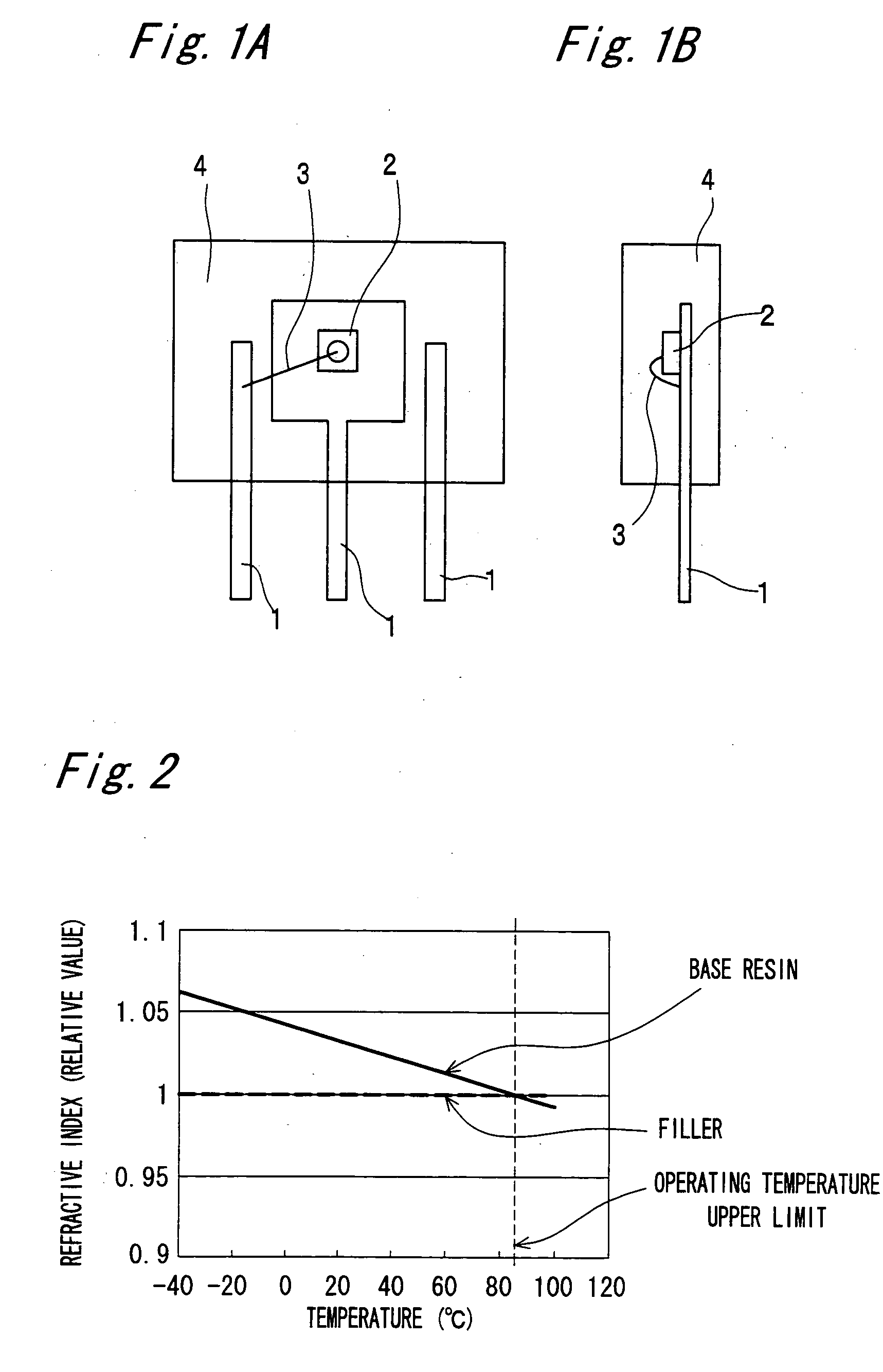
[0090]FIGS. 1A and 1B are views showing an optical semiconductor device of a first embodiment of the present invention. In detail, FIG. 1A is a front see-through view of the optical semiconductor device of the first embodiment, and FIG. 1B is a side see-through view of the optical semiconductor device of the first embodiment.

[0091] The optical semiconductor device has a lead frame 1, an LED 2 as one example of the optical semiconductor element, a wire 3 and a light-permeable mold resin 4 to which filler is added.

[0092] The wire 3 is constituted of a wire that has electrical conductivity, such as an Au wire, an Ag wire or an Al wire. Moreover, the mold resin 4 is formed by adding glass as filler to an epoxy resin. As the epoxy resin, various types of commercially available epoxy resins are usable. Also, as the glass filler, any type of commercially available glass filler is usable. Accordingly, the “epoxy resin” and the “glass filler” herein should not be interpreted as being limit...

second embodiment

[0113]FIGS. 6A and 6B are views showing an optical semiconductor device according to a second embodiment of the present invention. In detail, FIG. 6A is a front see-through view of the optical semiconductor device of the second embodiment, and FIG. 6B is a side see-through view of the optical semiconductor device of the second embodiment.

[0114] The optical semiconductor device of the second embodiment differs from the optical semiconductor device of the first embodiment essentially in that a photodiode (PD) 62, which is a photodetector, is adopted in place of the light-emitting element (LED) as the optical semiconductor element.

[0115] Regarding the optical semiconductor device of the second embodiment, no description will be provided for the same effects and advantages as those of the optical semiconductor device of the first embodiment and its modification examples, and only the construction and the effects and advantages different from those of the optical semiconductor device o...

third embodiment

[0119]FIGS. 7A and 7B are views showing an optical semiconductor device of a third embodiment of the present invention. In detail, FIG. 7A is a front see-through view of the optical semiconductor device of the third embodiment, and FIG. 7B is a side see-through view of the optical semiconductor device of the third embodiment.

[0120] The optical semiconductor device of the third embodiment differs from the optical semiconductor device of the first embodiment essentially in that a driving integrated circuit 76 for driving an LED 72 is provided.

[0121] Regarding the optical semiconductor device of the third embodiment, no description will be provided for the same construction and effects as those of the optical semiconductor device of the first embodiment and its modification examples, and only the construction and effects different from those of the optical semiconductor device of the first embodiment will be described.

[0122] The optical semiconductor device has a lead frame 71, an L...


PUM


Abstract

An optical semiconductor device has an optical semiconductor element (2) such as an LED or PD, and a light-permeable resin (4) encapsulating the optical semiconductor element. The light-permeable resin contains a base resin and filler. The light-permeable resin (4) has a characteristic that its transmittance increases with a temperature rise within an operating temperature range (e.g., −40° C.−+85° C.)

Description

[0001] This nonprovisional application claims priority under 35 U.S.C. §119(a) on Patent Application Nos. 2004-274695 and 2004-373537 filed in Japan on Sep. 22, 2004 and Dec. 24, 2004, respectively, the entire contents of which are hereby incorporated by reference. BACKGROUND OF THE INVENTION [0002] The present invention relates to an optical semiconductor device having an encapsulated optical semiconductor element, an optical communication device having the optical semiconductor device, and electronic equipment having the optical semiconductor device. [0003] Conventionally, as an optical semiconductor device having an optical semiconductor element that requires light transmission, or optical penetration, such as a light emitting diode (LED) and a photodiode (PD), products produced by using the transfer molding of a light-permeable mold resin are widely used. [0004] When a light-permeable mold resin is made of a single kind of resin mold material, there is an advantage that a partic...

Claims


Application Information

Patent Timeline
IPC IPC(8): H01L33/00H01L33/56
CPCG02B6/4212H01L31/0203H01L33/56H01L2224/48091H01L2224/48247H01L2224/45144H01L2224/45124H01L2924/00014H01L2924/00H01L2224/45139H01L2924/00011H01L2924/181H01L2924/01049H01L2924/00012H01L2224/45015H01L2924/207
Inventor OHE, NOBUYUKINAGURA, KAZUHITOTAKAKURA, HIDEYAKUSUDA, KAZUOSHOJI, HIROYUKI
Owner SHARP KK
Why Eureka
Try Eureka