Power amplifier for a transmitter

a power amplifier and transmitter technology, applied in the direction of amplifiers, amplifiers with semiconductor devices only, amplifiers, etc., can solve the problems of increasing the footprint and loss, difficult to realize the conventional power amplifiers by the coms technology, and difficult to realize the amplifiers of the gaas type and the inpgaas typ

Inactive Publication Date: 2006-03-30
SAMSUNG ELECTRONICS CO LTD
View PDF2 Cites 4 Cited by
  • Summary
  • Abstract
  • Description
  • Claims
  • Application Information

AI Technical Summary

Benefits of technology

[0013] Accordingly, the present invention has been made to solve at least the above-mentioned problems occurring in the prior art, and an object of the present invention is to provide a power amplifier for a transmitter, which can solve the above-mentioned problems of the prior art.

Problems solved by technology

It has been difficult to realize the conventional power amplifiers by the COMS technology because the power amplifiers based on the CMOS technology require relatively larger currents for obtaining a desired gain.
Other types of power amplifiers in the prior art consist of power amplifiers of GaAs (MESFET) and InPGaAs types which require relatively little current as compared with those of CMOS type but are expensive due to the lower yields thereof.
It is also difficult to realize the amplifiers of the GaAs type and the InPGaAs type in the form of Si system-on-chip because they are manufactured by using none-silicon materials.
It is still another problem that differential structures used in the GaAs and the InPGaAs employ discrete baluns outside of the structure, which increase the footprints and loss.
As described above, the conventional power amplifiers of the GaAs type and the InPGaAs type are expensive and have a low yield.
In the conventional power amplifiers of the CMOS type, it is difficult to obtain the necessary gain for a relevant current due to the low trans-conductance thereof.
Furthermore, the conventional power amplifiers generate considerable spurs (e.g., harmonics and IM—Intermodulation) although they are square-low devices.
Also, the conventional power amplifiers have a single-ended (antenna interface) structure, so that the conventional power amplifiers do not have sufficient voltage swings based on a fixed power supply voltage and thus fail to provide effective electrical power to the final output loads.
However, the output of the conventional power amplifier of the CMOS type is insufficient to satisfy the design specifications required in the mobile communication devices.
Further, in a state where the power amplifier of the single-in / out type prevails in the art, the power amplifier of the differential type which can be directly adapted to the outputs of an input stage transceiver (in the form of IC) is also problematic in that the voltage swing may half-reduce and consequently the saturation voltage may half-reduce.

Method used


Image

  • Power amplifier for a transmitter
  • Power amplifier for a transmitter
  • Power amplifier for a transmitter

Examples


Embodiment Construction

[0025] Hereinafter, preferred embodiments of the present invention will be described with reference to the accompanying drawings. In the following description, a detailed description of known functions and configurations incorporated herein will be omitted when it may make the subject matter of the present invention rather unclear.

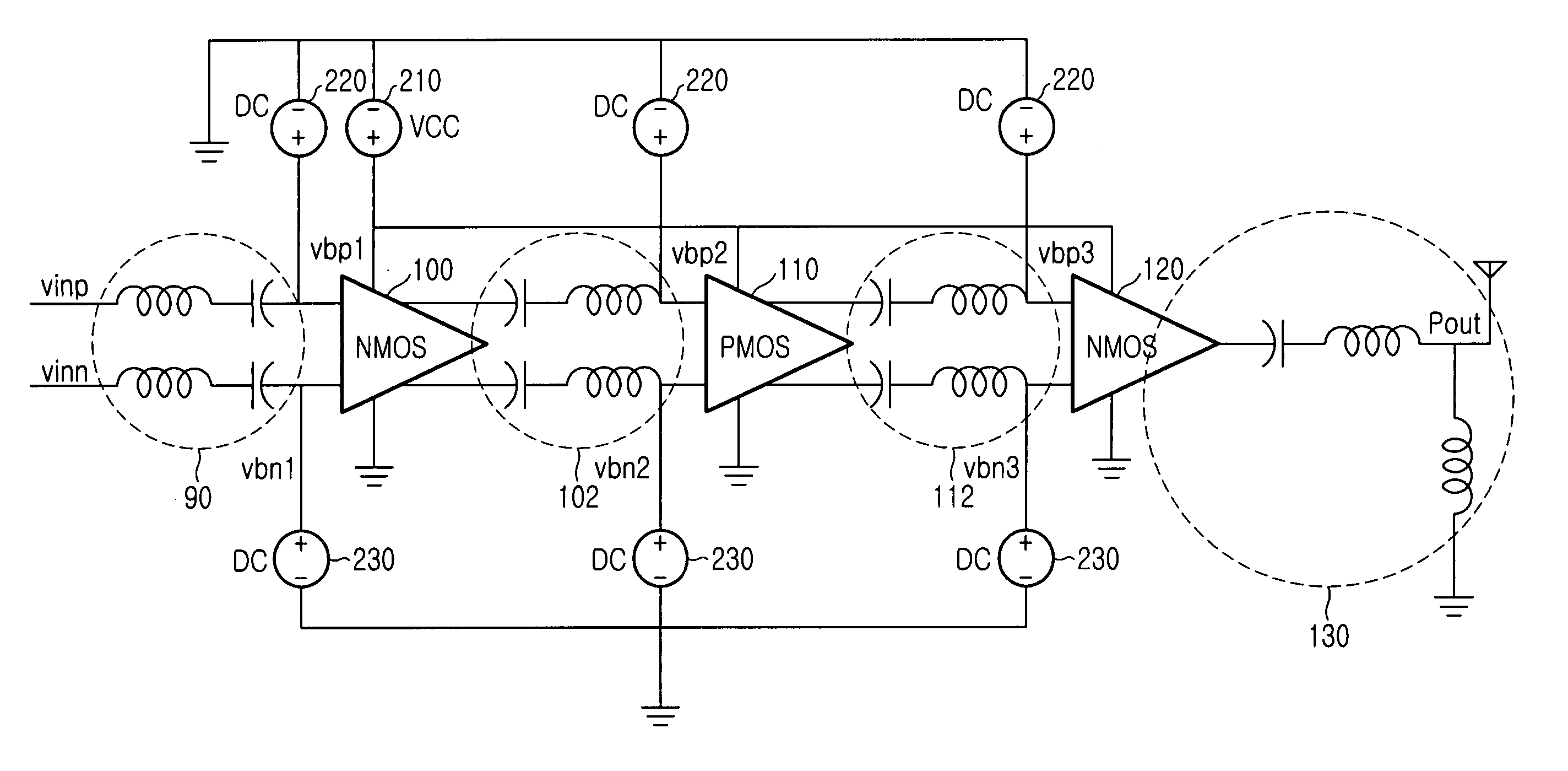
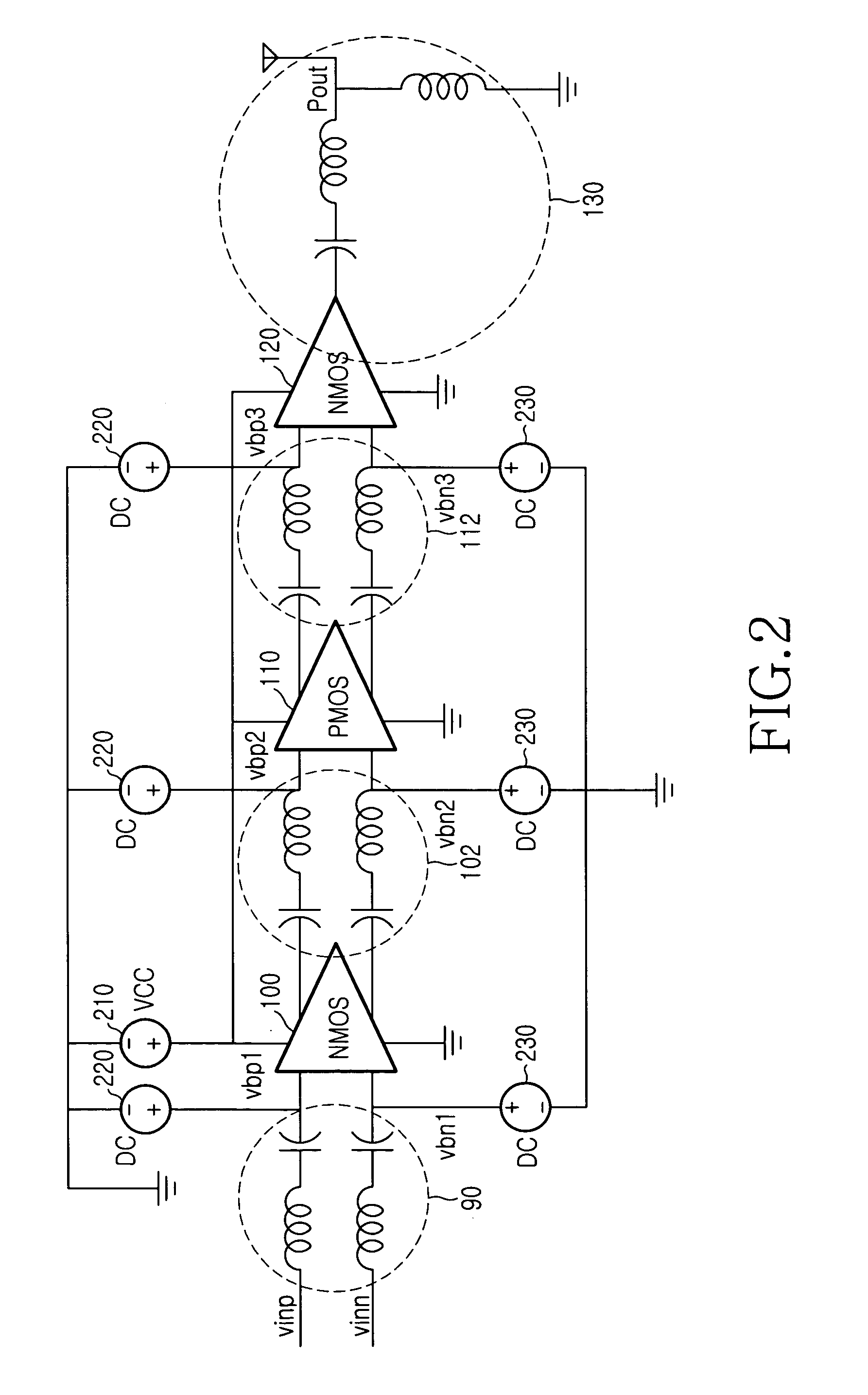
[0026]FIG. 2 is a schematic diagram of the power amplifier for the transmitter according to one embodiment of the present invention, and FIG. 3 is a schematic diagram of each stage in the power amplifier according to one embodiment of present invention.

[0027] The present invention provides a power amplifier having a Si-CMOS pseudo-differential structure. Referring to FIG. 2, the power amplifier according to an embodiment of the present invention includes three pseudo-differential amplifiers 100, 110 and 120 which correspond to an NMOS amplifier 100, a PMOS amplifier 110 and an NMOS amplifier 120. These three amplifiers 100, 110 and 120 are interlinked in...


PUM


Abstract

A power amplifier for a transmitter includes a plurality of CMOS amplifiers of different types which are serially and alternately connected, and matching circuits for matching impedance discrepancies between the CMOS amplifiers of different types.

Description

PRIORITY [0001] This application claims priority to an application entitled “POWER AMPLIFIER FOR A TRANSMITTER” filed in the Korean Industrial Property Office on Sep. 24, 2004 and assigned Serial No. 2004-77250, the contents of which are hereby incorporated by reference. BACKGROUND OF THE INVENTION [0002] 1. Field of the Invention [0003] The present invention relates to a terminal of a mobile communication system, and more particularly to a power amplifier for a transmitter of a mobile communication terminal. [0004] 2. Description of the Related Art [0005] A transmitter of a mobile communication terminal usually includes a power amplifier. CMOS (Complementary Metal-Oxide Semiconductor) technology has enabled on-chip integration of the power amplifier, which has made a contribution to minimize BOM (Build on Materials) and areas for mounting devices (i.e., footprints). Also, the on-chip integration technology of the power amplifier has allowed not only for the elimination of the requi...

Claims


Application Information

Patent Timeline
Patent Type & Authority Applications(United States)
IPC IPC(8): H03F3/191
CPCH03F1/565H03F3/191H03F3/193H03F3/45179H03F2203/45652H03F3/68H03F2203/45464H03F2203/45638H03F3/45475H03F3/20
Inventor SIM, DAE-HYUN
Owner SAMSUNG ELECTRONICS CO LTD
Why Eureka
Try Eureka