Solid-state image pickup device and method of resetting the same

a solid-state image and pickup device technology, applied in the field of solid-state image pickup devices, can solve the problems of low manufacturing yield, affecting the variance of manufacturing process, saturation charge qsub>sat/sub>or the depletion voltage vsub>dp /sub>, etc., to achieve effective photoelectric conversion, reduce residual charge

Inactive Publication Date: 2006-03-30
CANON KK
View PDF5 Cites 16 Cited by
  • Summary
  • Abstract
  • Description
  • Claims
  • Application Information

AI Technical Summary

Benefits of technology

[0018] Therefore, it is an object of the present invention to provide a solid-state image pickup device that can effectively reduce the residual charge in the photoelectric converter and operate effectively and efficiently for photoelectric conversion and also a method of resetting the same.
[0019] Another object of the present invention is to expand the process tolerance for manufacturing a solid-state image pickup device that is adapted to be reset in a desired manner.

Problems solved by technology

On the other hand, it is rather difficult for an APS to reduce the chip size that is a determinant of the dimensions of its optical system because of the large number of elements it has for each pixel.
However, the saturation charge Qsat or the depletion voltage Vdp is apt to be affected by variances of the manufacturing process.
Then, the net result is a low manufacturing yield.

Method used


Image

  • Solid-state image pickup device and method of resetting the same
  • Solid-state image pickup device and method of resetting the same
  • Solid-state image pickup device and method of resetting the same

Examples


embodiment 1

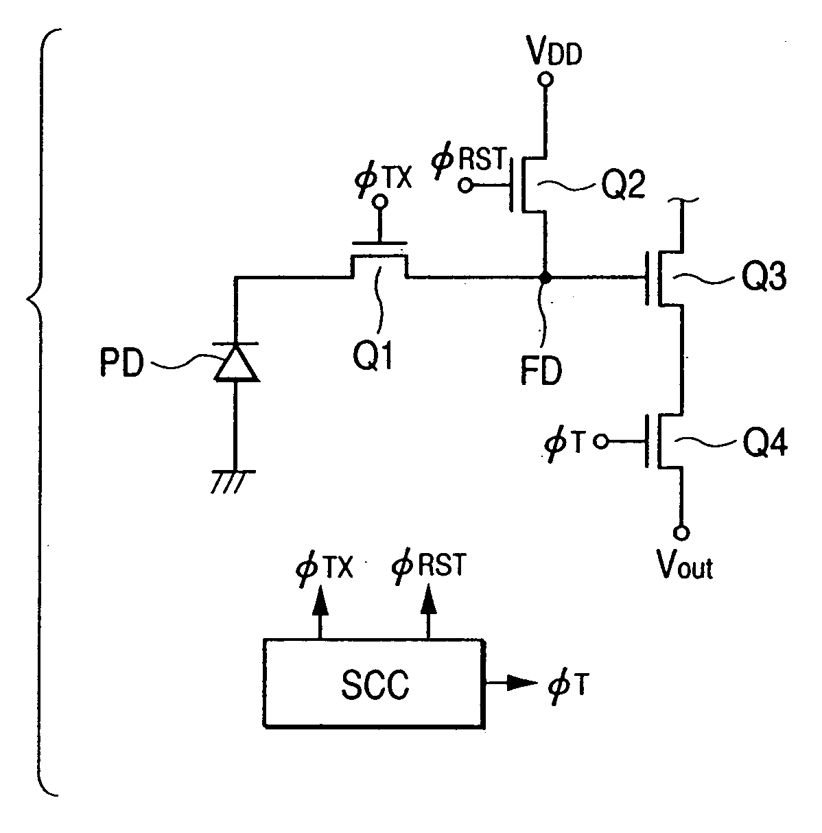
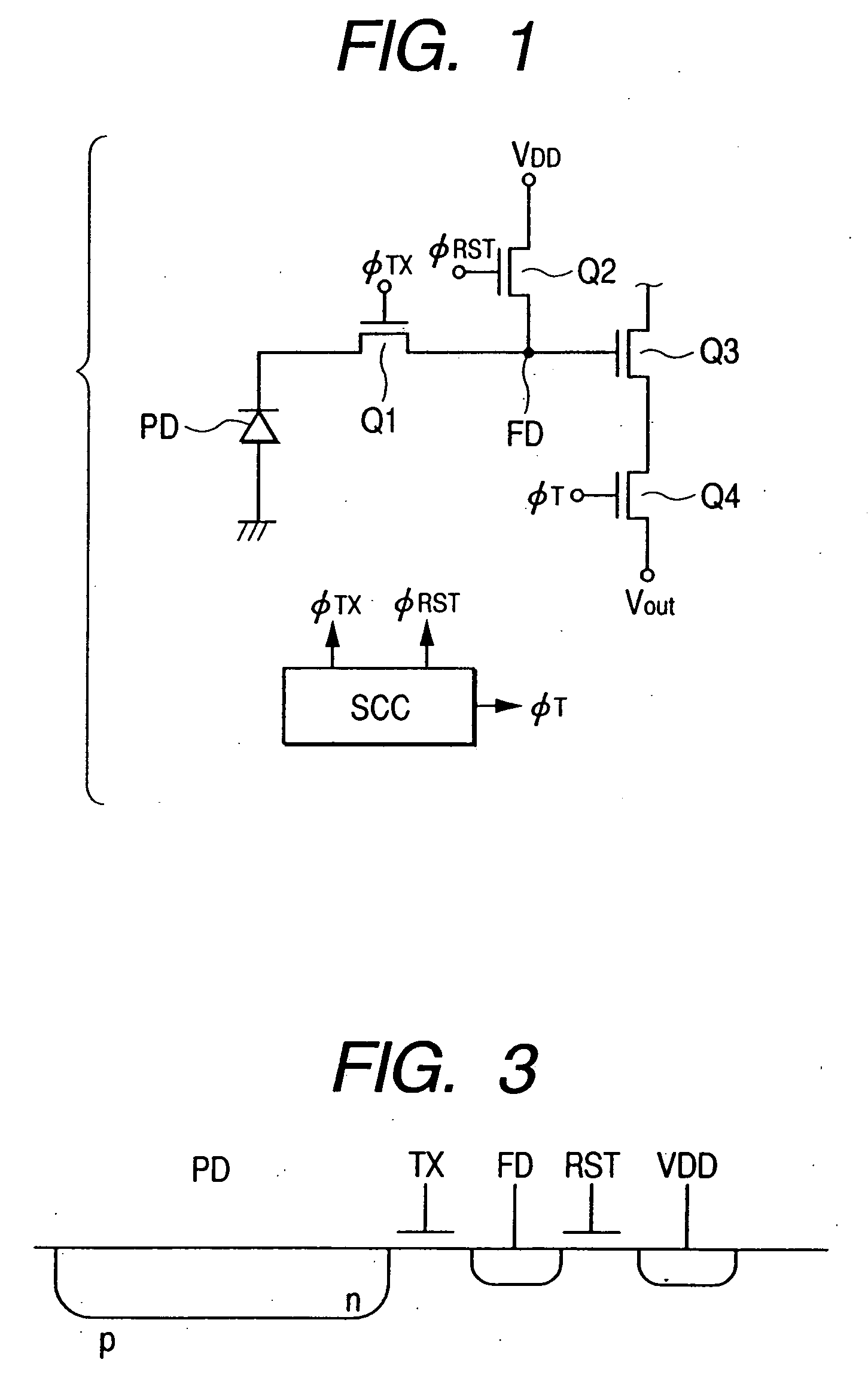
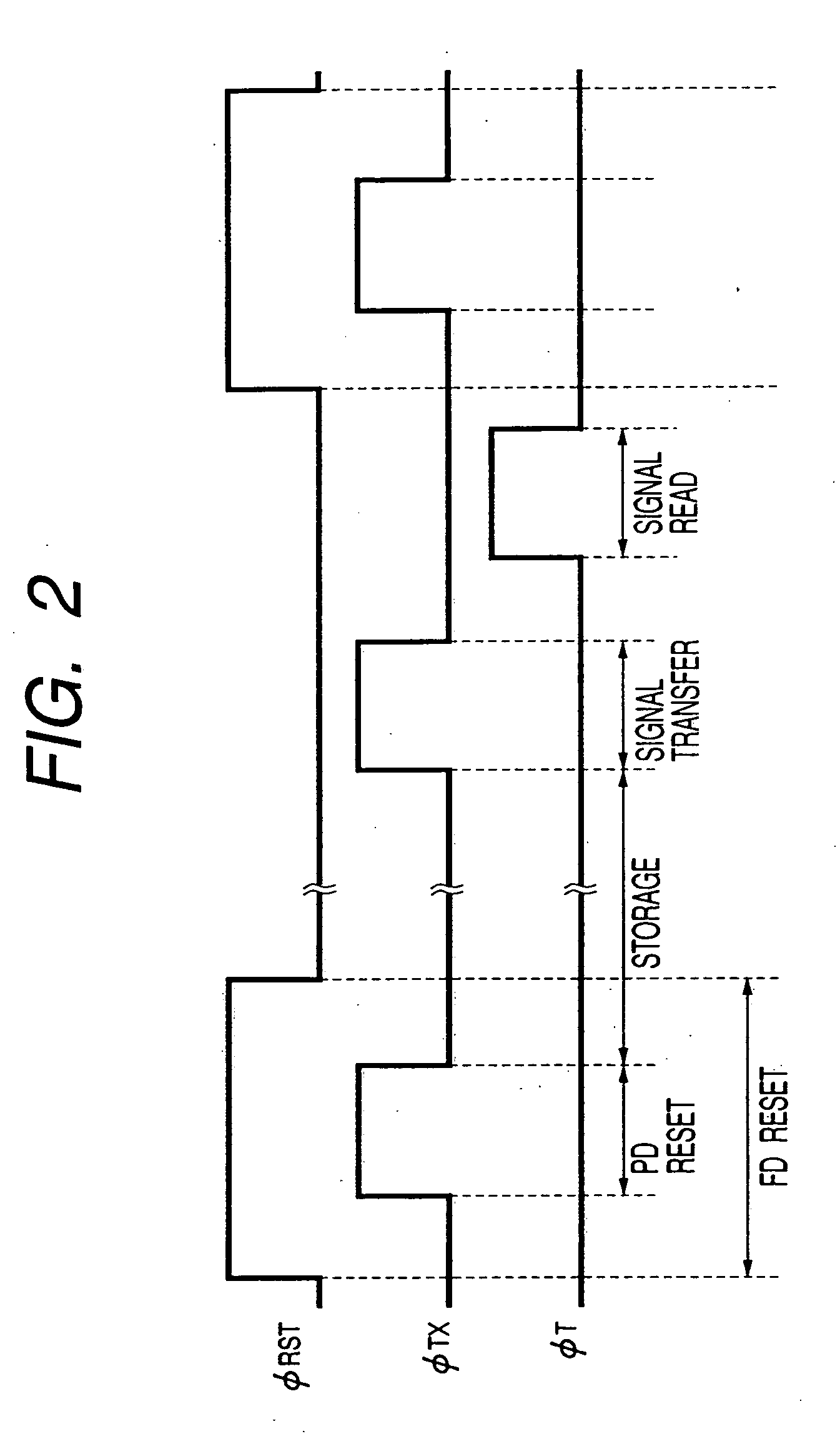
[0046]FIG. 1 is a schematic circuit diagram of a pixel of a preferred embodiment of solid-state image pickup device according to the invention and FIG. 2 is a drive timing chart illustrating the operation of the preferred embodiment of solid-state image pickup device according to the invention. Note that the basic configuration of this embodiment is commonly applicable to the remaining embodiments as will be described hereinafter.

[0047] The photoelectric converter PD typically comprises a photodiode having a PN junction or a PIN junction. One of the terminals of the photoelectric converter is held to a reference potential for applying a reverse bias voltage, while the other terminal thereof is connected to a transfer switch Q1. From FIG. 1, it will be seen that the cathode is connected to the transfer switch Q1 to transfer electrons.

[0048] In FIG. 1, Q2 denotes a reset switch having one of its terminals connected to reference voltage source VDD for applying a resetting voltage.

[0...

embodiment 2

[0071] Now, another embodiment of the present invention will be described by referring to FIGS. 6, 7 and 8.

[0072]FIG. 6 is a schematic cross sectional view of the second embodiment of solid-state image pickup device according to the invention. FIG. 7 is a schematic illustration of changes that can take place in the potential profiles of principal sections of the embodiment of solid-state image pickup device of FIG. 6. FIG. 8 is a drive timing chart illustrating the operation of the preferred embodiment of solid-state image pickup device of FIG. 6. Note that the embodiment of solid-state image pickup device of FIG. 6 has a basic circuit configuration same as the embodiment of FIG. 1.

[0073] Referring to FIG. 6, the photodiode of the photoelectric converter of this embodiment is a buried type photodiode comprising a P-type well 101 formed in the substrate surface, a N-type region 105 and a surface p-region 104. As described above, with a buried type photodiode, the dark current that ...

embodiment 3

[0082]FIG. 9 is an equivalent circuit diagram of a pixel of the solid-state image pickup device according to the invention. In FIG. 9, the photodiode PD is a buried type photodiode as in the case of the preceding embodiments. Otherwise, there are shown a MOS transistor Q1 operating as transfer switch for transferring a photoelectric charge to floating diffusion region FD, a MOS transistor Q2 operating as reset switch for resetting the floating diffusion region FD, an input MOS transistor Q3 of a source follower for outputting the voltage of the floating diffusion region FD and a MOS transistor Q4 operating as selection switch for selecting a pixel. The input MOS transistor Q3 of the source follower takes the role of a signal amplifier and the floating diffusion region FD operates as the input terminal of this signal amplifier.

[0083]FIG. 10 is a schematic circuit diagram of a solid-state image pickup device comprising a matrix of 2×2 pixels PX, each having a circuit configuration as...


PUM


Abstract

A solid-state image pickup device comprises for each pixel a photoelectric converter PD, an input terminal FD of a signal amplifier and a transfer switch TX for transferring an optical signal from the photoelectric converter to the input terminal. The device additionally comprises means for resetting the photoelectric converter by opening the transfer switch TX under a condition of holding the voltage of the input terminal FD to a fixed high level before storing the optical signal in the photoelectric converter PD. With this arrangement, any residual electric charge in the photoelectric converter can be eliminated without paying the cost of reducing the manufacturing yield and degrading the chip performance.

Description

BACKGROUND OF THE INVENTION [0001] 1. Field of the Invention [0002] This invention relates to a solid-state image pickup device to be used for an image input apparatus such as a digital camera, a video camera, an image scanner or an AF sensor and also to a method of resetting the same. [0003] 2. Related Background Art [0004] Typical examples of solid-state image pickup device include the CCD image sensor and the non-CCD image sensor. The former comprises a photoelectric converter having photodiodes and a CCD shift register, whereas the latter comprises a photoelectric converter having photodiodes or photo-transistors and a scanning circuit having MOS transistors. [0005] The APS (active pixel sensor) is a type of non-CCD image sensor comprising a photodiode and MOS transistors. [0006] More specifically, an APS comprises combinations of a photodiode, a MOS switch and an amplifier for amplifying the signal from the photodiode, each combination being arranged in correspondence to a pixe...

Claims


Application Information

Patent Timeline
Patent Type & Authority Applications(United States)
IPC IPC(8): H04N5/335H04N5/359
CPCH04N5/238H04N5/3597H04N5/353H04N23/75H04N25/53H04N25/626
Inventor KOIZUMI, TORUSUGAWA, SHIGETOSHIKOCHI, TETSUNOBU
Owner CANON KK
Why Eureka
Try Eureka