Methods of forming a thin layer for a semiconductor device and apparatus for performing the same

a technology of semiconductor devices and thin layers, applied in the direction of coatings, chemical vapor deposition coatings, metallic material coating processes, etc., can solve the problems of reducing device reliance, short circuit between conductive structures, and problematic seam defects, so as to achieve sufficiently improved flow characteristics and gap-fill characteristics of insulation layers, seam defects are remarkably reduced

Inactive Publication Date: 2006-03-30
SAMSUNG ELECTRONICS CO LTD
View PDF10 Cites 65 Cited by
  • Summary
  • Abstract
  • Description
  • Claims
  • Application Information

AI Technical Summary

Benefits of technology

[0021] According to some embodiments of the present invention, a flow characteristic and a gap-fill characteristic of the insulation layer are sufficiently improved, so that a seam defect is remarkably decreased when the recessed portion is filled with the insulation layer.

Problems solved by technology

However, there is a problem that the above silicon oxide (SiO2) layer may include a seam defect, and the seam defect can be problematic in a subsequent process.
That is, an etchant in a subsequent wet etching process may enlarge the seam defect on the SiO2 layer, and a conductive material may be filled into the enlarged seam defect, thereby potentially generating a short circuit between conductive structures in a semiconductor device, and a reliance reduction of a device.
However, it is believed that the above suggestions may not provide a solution to the problems in that the CVD process may be difficult to control due to a low processing temperature and an additional unit may be useful for generating the plasma and microwaves.

Method used


Image

  • Methods of forming a thin layer for a semiconductor device and apparatus for performing the same
  • Methods of forming a thin layer for a semiconductor device and apparatus for performing the same
  • Methods of forming a thin layer for a semiconductor device and apparatus for performing the same

Examples


Embodiment Construction

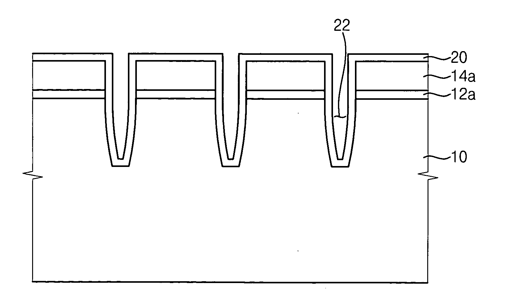
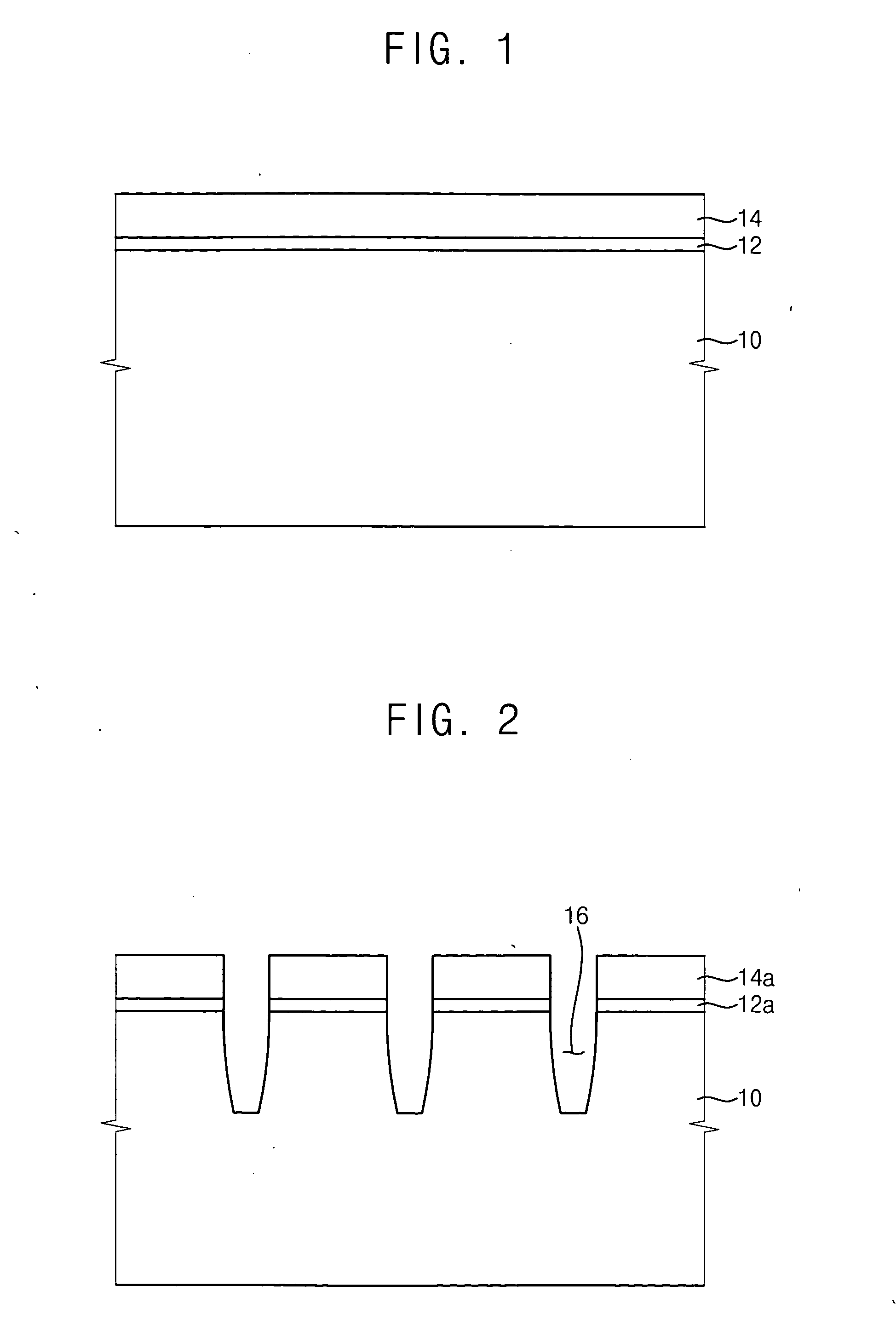
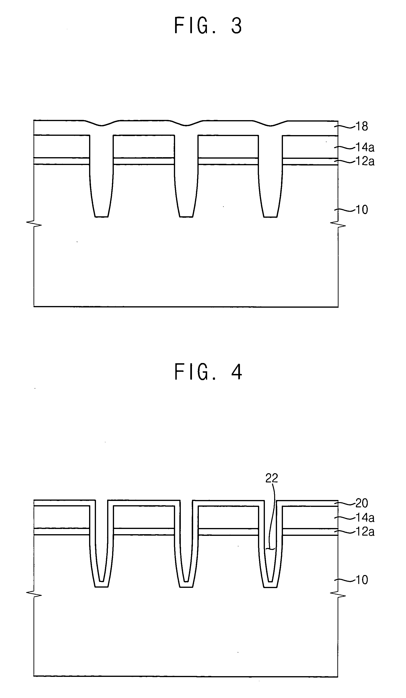
[0035] The invention is described more fully hereinafter with reference to the accompanying drawings, in which embodiments of the invention are shown. This invention may, however, be embodied in many different forms and should not be construed as limited to the embodiments set forth herein. Rather, these embodiments are provided so that this disclosure will be thorough and complete, and will fully convey the scope of the invention to those skilled in the art. In the drawings, the size and relative sizes of layers and regions may be exaggerated for clarity.

[0036] It will be understood that when an element or layer is referred to as being “on”, “connected to” or “coupled to” another element or layer, it can be directly on, connected or coupled to the other element or layer or intervening elements or layers may be present. In contrast, when an element is referred to as being “directly on,”“directly connected to” or “directly coupled to” another element or layer, there are no interveni...


PUM

PropertyMeasurementUnit
temperatureaaaaaaaaaa
internal pressureaaaaaaaaaa
pressureaaaaaaaaaa

Abstract

The present invention can provide methods of forming a thin layer for a semiconductor device. The methods can include forming a recessed portion on an object, and forming an insulation layer on the object by reacting a water vapor, an oxygen gas including an oxygen radical and an organic silicon source gas with each other, so that the recessed portion is filled with the insulation layer. Accordingly, a flow characteristic of the insulation layer can be improved, so that a seam defect can be sufficiently decreased in the insulation layer. The present invention can further provide apparatus for forming a thin layer.

Description

CROSS REFERENCE TO RELATED APPLICATION [0001] This application claims priority under 35 USC §119 to Korean Patent Application No. 10-2004-71253 filed on Sep. 7, 2004, the content of which is herein incorporated by reference in its entirety. FIELD OF THE INVENTION [0002] The present invention relates to methods of forming a thin layer for a semiconductor device and an apparatus for performing the same. More particularly, the present invention relates to methods of forming a thin layer for a semiconductor device using a chemical vapor deposition (CVD) process and apparatus for performing the same. BACKGROUND OF THE INVENTION [0003] Recently, as information media, such as computers, are widely used, the semiconductor industry has made great strides. In a functional aspect, it is desirable that a semiconductor device operate at a high speed and maintain large storing capacitance. Accordingly, there is a need in the semiconductor technology is developed to improve the integration degree,...

Claims


Application Information

Patent Timeline
Patent Type & Authority Applications(United States)
IPC IPC(8): H01L21/31
CPCC23C16/402H01L21/02164H01L21/02214H01L21/02238H01L21/02255H01L21/02271H01L21/02274H01L21/76H01L21/762
Inventor BAEK, EUN-KYUNGNA, KYU-TAERHA, SANG-HO
Owner SAMSUNG ELECTRONICS CO LTD
Why Eureka
Try Eureka