

Gas diffusion plate and manufacturing method for the same
Inactive Publication Date: 2006-04-06
COVALENT MATERIALS CORP
View PDF7 Cites 43 Cited by
- Summary
- Abstract
- Description
- Claims
- Application Information
AI Technical Summary
Benefits of technology
[0012] The invention was carried out in view of the above-mentioned situations and intends to provide a gas diffusion plate in which yttria excellent in the plasma resistance and the halogen gas resistance is solidly applied over all surfaces of a gas discharge hole disposed to an alumina base material or an aluminum base material, a material inside of the gas discharge hole is inhibited from being etched owing to the discharge to generate particles, and thereby a manufacturing yield of semiconductor can be improved, and that is less expensive; and a manufacturing method thereof.
[0044] According to the gas diffusion plate as set forth the invention, since the invention is achieved by taking above-mentioned situations into considerations, a gas diffusion plate in which yttria excellent in the plasma resistance and the halogen gas resistance is solidly applied over all surface of a gas discharge hole disposed to an alumina base material or an aluminum base material. Accordingly, a material inside of the gas discharge hole is inhibited from being etched which is occurred by the discharge and the generation of particles therefrom is also prevented. Since the generation of particles is prevented, a manufacturing yield of semiconductor can be improved. Also, a manufacturing method for the gas diffusion plate in less expensive can be provided.
Problems solved by technology
However, in such a plasma processor where plasma is generated between the wafer and the shower plate to apply the etching, not only the wafer but also the shower plate itself is etched, thereby particles are generated, resulting in lowering the manufacturing yield of semiconductor devices.
Accordingly, there is a problem with durability.
In addition, because yttria and YAG are more expensive than an alumina base material and an aluminum base material, a thermal spray coating is formed on the alumina base material or the aluminum base material to improve the corrosion resistance of the surface thereof.
However, in the shower plate on which an yttria thermal spray coating is formed, since the yttria thermal spray coating does not reach onto an inner wall portion of the gas discharge hole, it is difficult to form an yttria thermal spray coating on the wall surface of the hole.
Furthermore, if it could be applied, the thermal spray coating has poor adhesiveness and can be easily peeled off.
However, when the thermal spraying material is obliquely thermal sprayed on an inner surface of the gas discharge hole, excellent adhesiveness is not obtained.
Accordingly, inconveniences such as the peeling and particle generation are caused.
Still furthermore, when a bulk of yttria is directly adhered with an adhesive, since the adhesive includes an organic binder, there is a problem in that a gas caused by the organic binder is generated.
In addition, there is still another problem in high cost because of the additional adhering process.
However, since it is poorer in the strength than the alumina base material or aluminum base material, there is a problem in that the thermal stress during use of the gas diffusion plate may cause its breakage.
In addition, the cost regarding the process of single yttria is high, in particular, the larger the dimension is, the higher the cost becomes.
Method used
View moreImage
Smart ImageViewing Examples

Examples
examples
[0074] [Test 1]
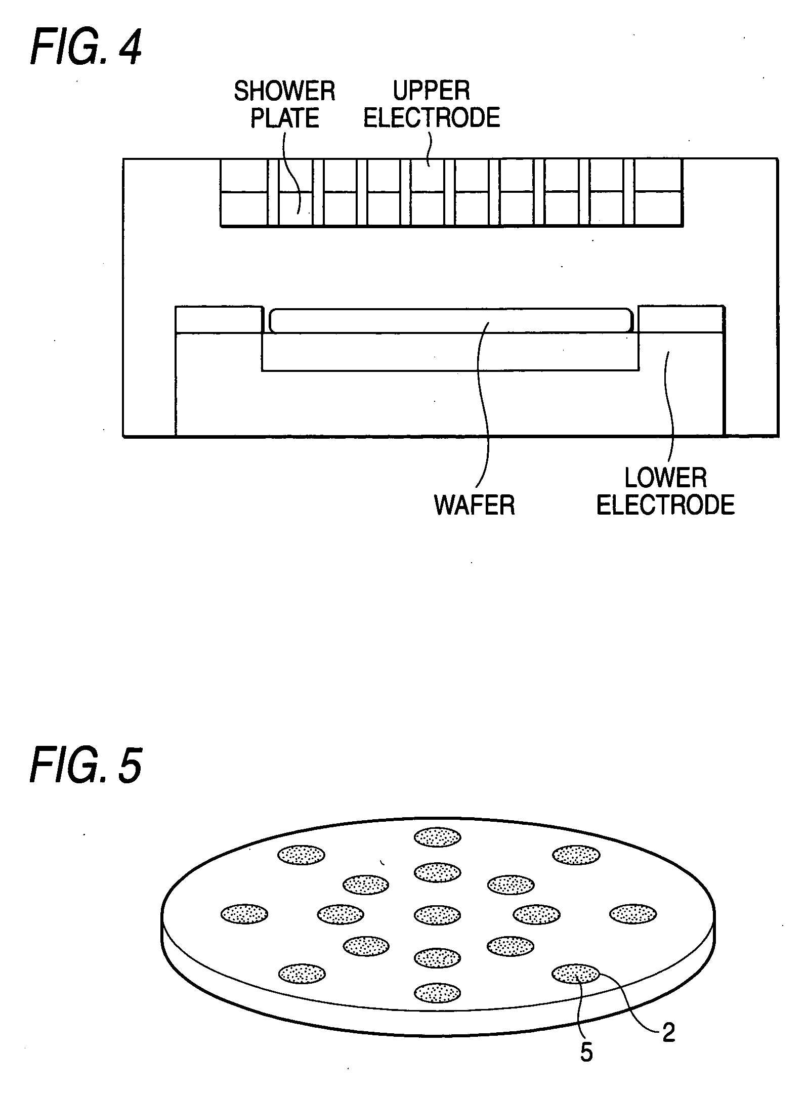
[0075] As shown in FIG. 4, a shower plate according to the invention was installed in a semiconductor etcher, a semiconductor wafer was set at a position lower than the shower plate, a plasma gas of CF4+He+Ar was introduced from the shower plate, followed by discharging, and particles on the wafer were counted.
example 1
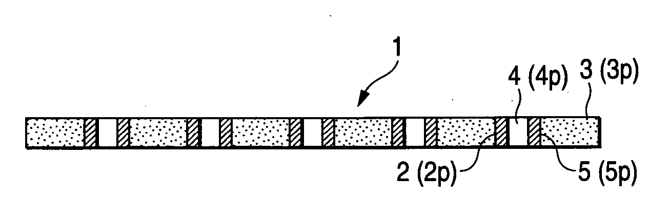
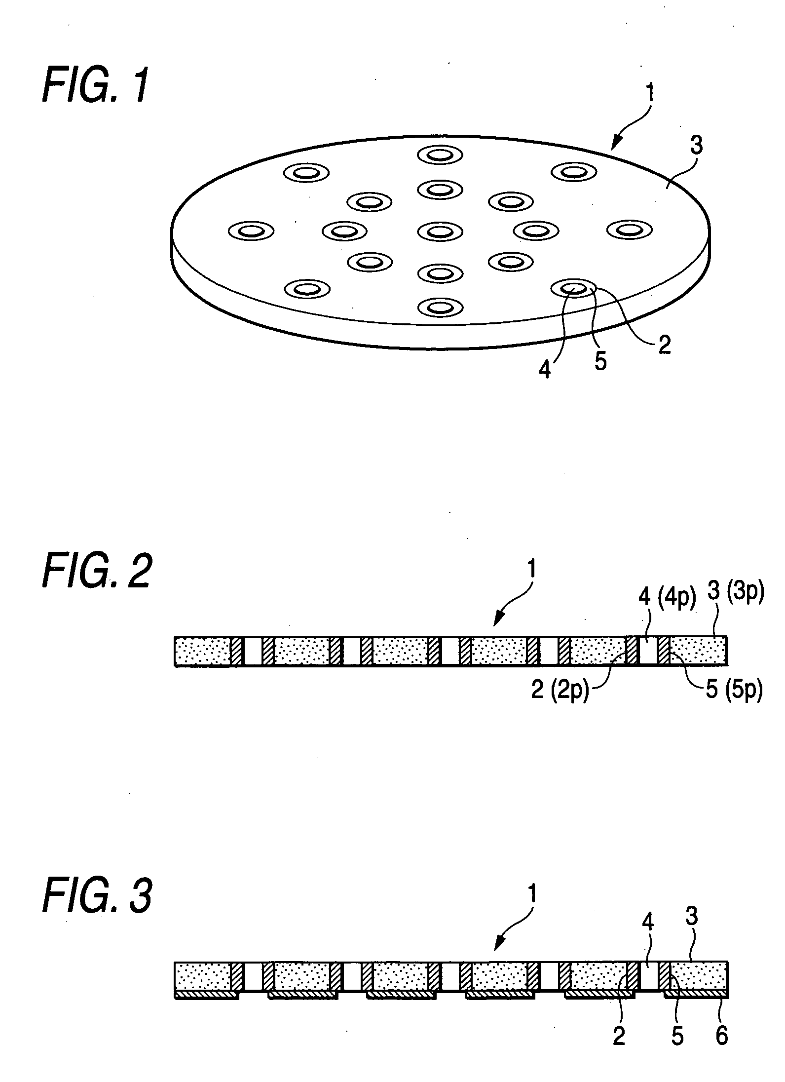
[0076] A shower plate in which a cylindrical yttria pipe was shrink-fitted in a circular through hole of a disk-like alumina base material such as shown in FIG. 1.
example 2
[0077] A shower plate in which an yttria thermal spray coating is applied to an exposed portion, which is exposed to a corrosive gas, of the alumina base material of the Example 1 as shown in FIG. 2.
Login to View More PUM
 Abstract
Description
[0001] The present invention claims foreign priority to Japanese patent application No. P.2004-288041, filed on Sep. 30, 2004, P.2004-349946, filed on Dec. 2, 2004, and P.2005-242206, filed on Aug. 24, 2005, the contents of which are incorporated herein by reference. BACKGROUND OF THE INVENTION [0002] 1. Field of the Invention [0003] The present invention relates to a gas diffusion plate and a manufacturing method for the same, in particular, a gas diffusion plate in which a cylindrical yttria pipe is shrink-fitted to a circular through hole disposed to an alumina base material or an aluminum base material and a manufacturing method for the same. [0004] 2. Description of the Background Art [0005] In a manufacturing process of a semiconductor device, in order to apply a desired process on a surface of a wafer, a plasma processor is employed. This kind of the plasma processor has an upper electrode disposed in an upper portion of a chamber and called also a shower plate. The shower pl...
Claims
Login to View More Application Information
Patent Timeline
 IPC IPC(8): C25D1/08B32B15/00B32B15/01
CPCC22C21/00C23C4/105C25D1/08Y10T428/12493H01J37/32495Y10T428/12736Y10T428/12361H01J37/3244C23C4/11H01L21/00
InventorWATANABE, KEISUKEMORITA, KEIJINAGASAKA, SACHIYUKI
OwnerCOVALENT MATERIALS CORP