Memory structure and manufacturing as well as programming method thereof

a memory structure and manufacturing technology, applied in the field of nonvolatile memory, to achieve the effect of flexible operation of floating gate memory cells and significant increase in memory structure density

Inactive Publication Date: 2006-04-06
SKYMEDI CORPORATION
View PDF3 Cites 8 Cited by
  • Summary
  • Abstract
  • Description
  • Claims
  • Application Information

AI Technical Summary

Benefits of technology

[0015] The method of the present invention uses F-N programming instead of hot electron programming. It provides an alternative operation method so that the more flexible operation for floating gate memory cells in this memory structure can be attained. Moreover, hot electron and F-N programming in nitride gate can be achieved, which increases the memory structure density significantly.

Problems solved by technology

Apparently, the above prior art references are either complex or limited to the operation by hot electron programming, so that an alternative process and operation method are needed to enhance the production efficiency and obtain better operation flexibility.

Method used


Image

  • Memory structure and manufacturing as well as programming method thereof
  • Memory structure and manufacturing as well as programming method thereof
  • Memory structure and manufacturing as well as programming method thereof

Examples


first embodiment

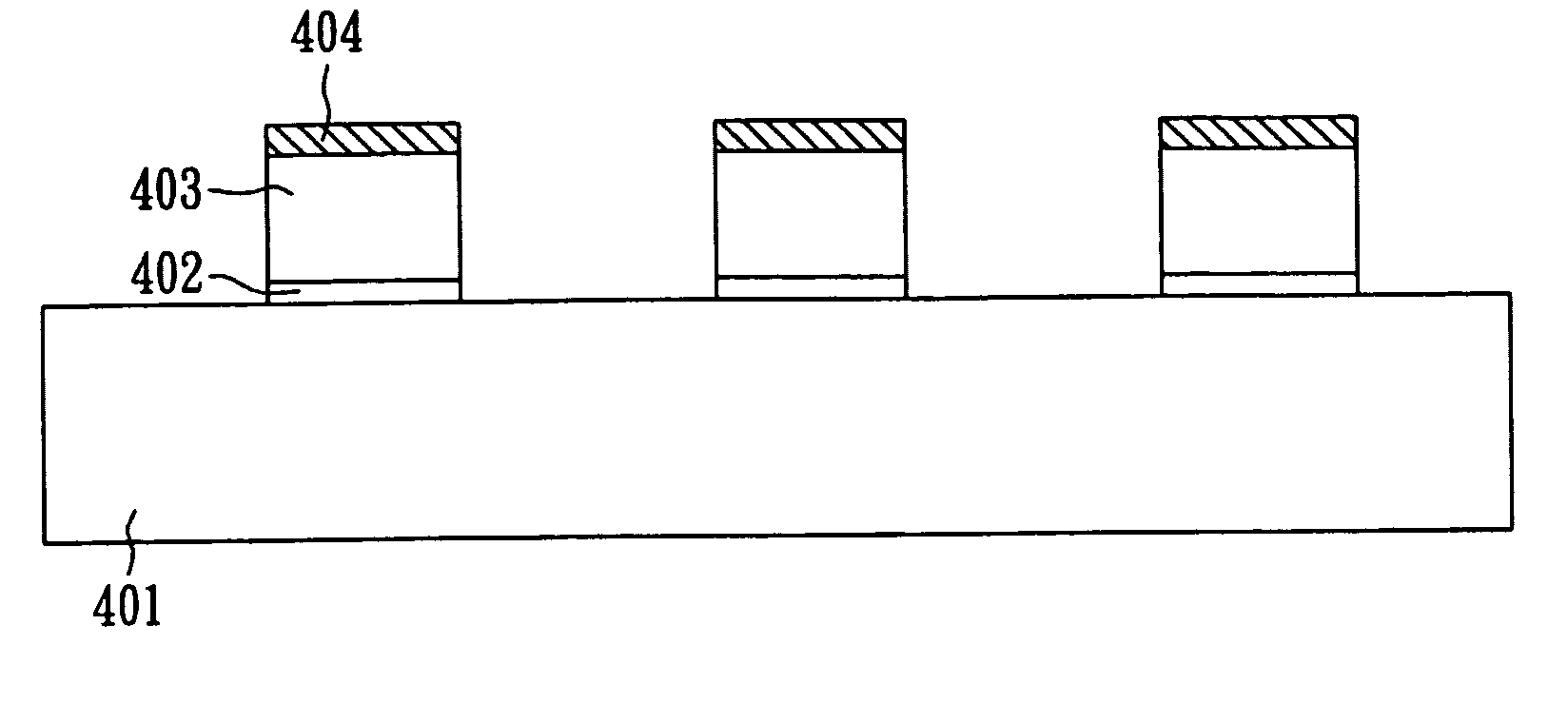
[0024] FIGS. 4(a) through 4(f) illustrate a process for forming the memory structure of the first embodiment in accordance with the present invention.

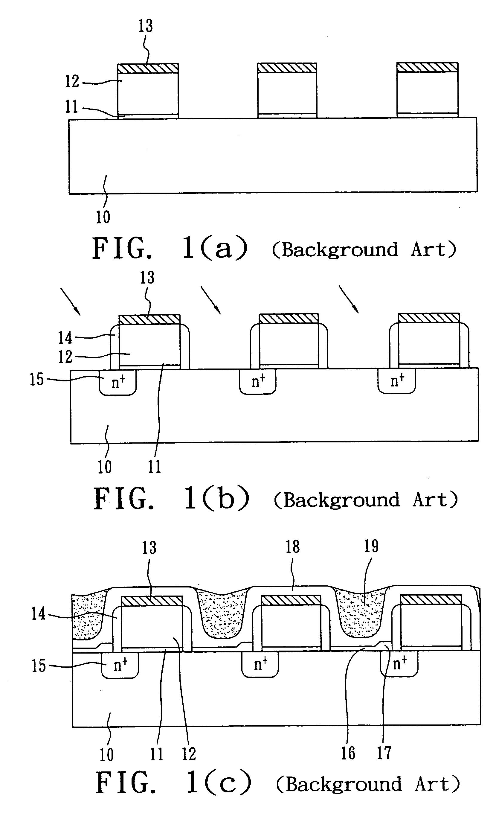
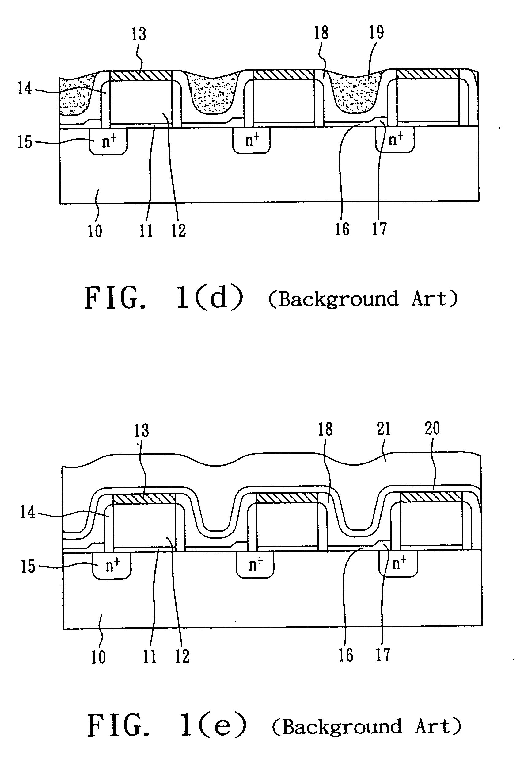
[0025] In FIG. 4(a), an ONO layer, a first conductive layer, an insulating layer are sequentially formed on a silicon substrate 401, and are patterned to be individual gate structures afterwards. Each gate structure comprises an ONO layer 402, a first conductive line 403 and an insulating layer 404. The first conductive line 403 may be composed of polysilicon, whereas the insulating layer 404 may be a multilayer of silicon nitride and silicon oxide. In FIG. 4(b), dielectric spacers 405 ranging from 100 to 300 angstroms and mask spacers 407, e.g., silicon nitride spacers, ranging from 200 to 800 angstroms are sequentially formed beside the first conductive lines 403. Then, photoresist is deposited and patterned as multiple photoresist caps 406 to cover one side mask spacer 407 of each first conductive line 403, and in consequence, as sh...

second embodiment

[0037] FIGS. 5(a) through 5(f) illustrate a process for forming the memory structure of the second embodiment in accordance with the present invention.

[0038] In FIG. 5(a), a gate dielectric layer, a first conductive layer and a silicon nitride layer are sequentially formed on a semiconductor substrate 501, and are patterned to be separated gate structures. Each gate structure comprises a gate dielectric layer 502, a first conductive line 503 and a silicon nitride layer 504, where the gate dielectric layer 502 is in the range of 70 to 150 angstroms, the first conductive line 503 is in the range of 400 to 2000 angstroms, and the silicon nitride layer 504 is in the range of 500 to 2000 angstroms. Then, dielectric spacers 506 ranging from 100 to 300 angstroms are formed beside the two sides of the first conductive line 503, followed by tilt-implanting dopants such as arsenic ions with an energy between 5×10¹⁴ and 5×10¹⁵ atoms / cm2, so as to form doping regions 505 serving as bitlines. In...


PUM


Abstract

A memory structure includes a floating gate and a nitride gate dielectric on a semiconductor substrate, wherein the floating gate and nitride gate dielectric function as two memory cells. In addition to the floating gate and nitride gate dielectric, the memory structure further comprises two bitlines and a select gate. The two bitlines are formed in the semiconductor substrate, the floating gate and the select gate are formed above the semiconductor substrate and transversely disposed between the two bitlines, and the nitride gate dielectric is formed between the select gate and the semiconductor substrate.

Description

BACKGROUND OF THE INVENTION [0001] (A) Field of the Invention [0002] The present invention is related to a non-volatile memory and a manufacturing method as well as a programming method thereof, and more specifically to a memory structure including a split gate and the relevant manufacturing and programming method thereof. [0003] (B) Description of the Related Art [0004] Non-volatile memory devices are currently in wide use in electronic components that require the retention of information when electrical power is terminated. Non-volatile memory devices include read only memory (ROM), programmable read only memory (PROM), erasable programmable read only memory (EPROM) and electrically erasable programmable read only memory (EEPROM) devices. EEPROM devices differ from other non-volatile memory devices in that they can be electrically programmed and erased. Flash EEPROM devices are similar to EEPROM devices in that memory cells can be programmed and erased electrically. However, flash...

Claims


Application Information

Patent Timeline
Patent Type & Authority Applications(United States)
IPC IPC(8): H01L21/44
CPCH01L27/115H01L27/11521H10B69/00H10B41/30
Inventor SHONE, FUJA
Owner SKYMEDI CORPORATION
Why Eureka
Try Eureka