Method and apparatus for the depth-resolved characterization of layer of a carrier

a carrier and depth resolution technology, applied in the field of apparatus and method for the depth resolution characterization of the carrier layer, can solve the problem of local destruction of the carrier and achieve the effect of high accuracy

Inactive Publication Date: 2006-04-13
POLARIS INNOVATIONS
View PDF4 Cites 12 Cited by
  • Summary
  • Abstract
  • Description
  • Claims
  • Application Information

AI Technical Summary

Benefits of technology

[0014] The present invention provides an improved method and apparatus which enab

Problems solved by technology

Furthermore, the carrier is locally destroye

Method used


Image

  • Method and apparatus for the depth-resolved characterization of layer of a carrier
  • Method and apparatus for the depth-resolved characterization of layer of a carrier
  • Method and apparatus for the depth-resolved characterization of layer of a carrier

Examples


Embodiment Construction

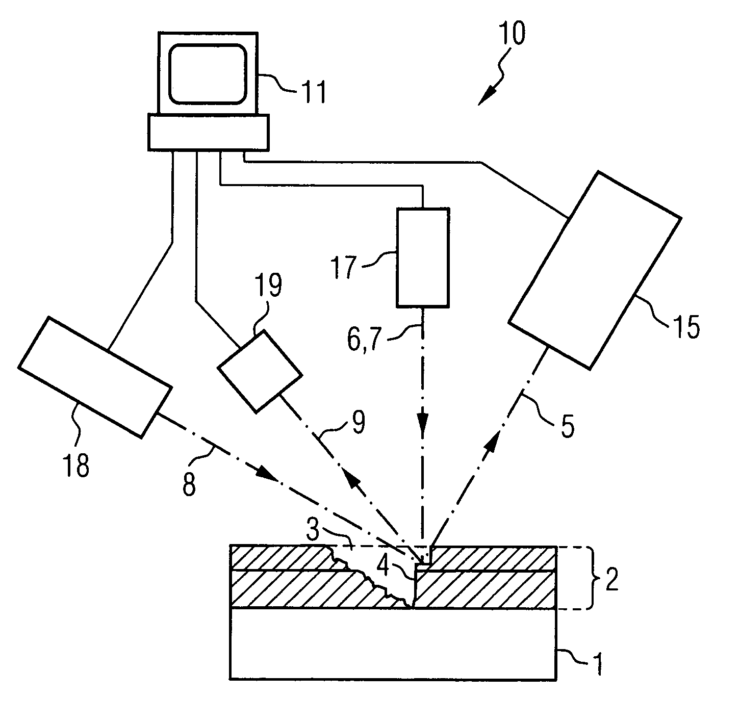
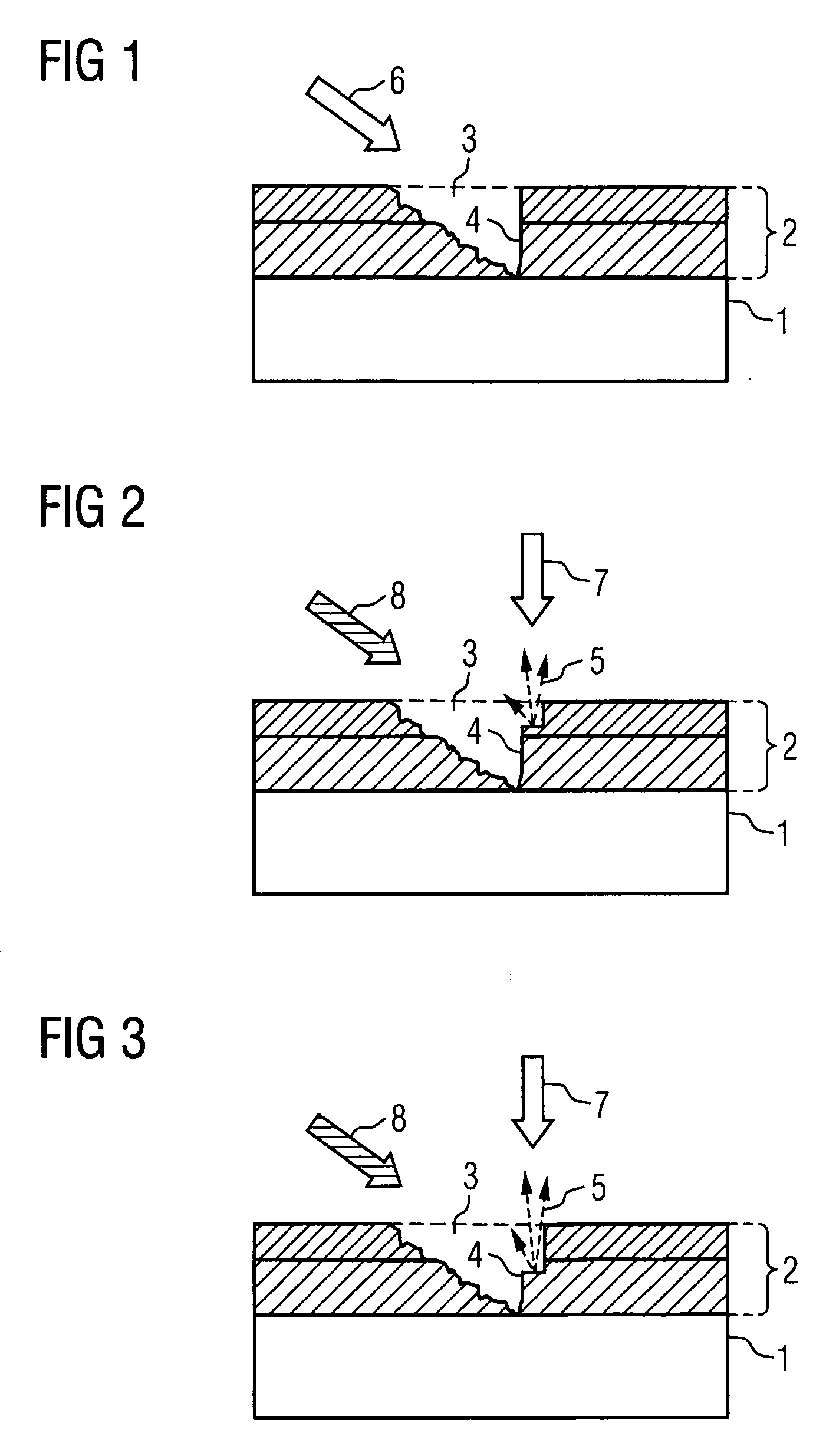
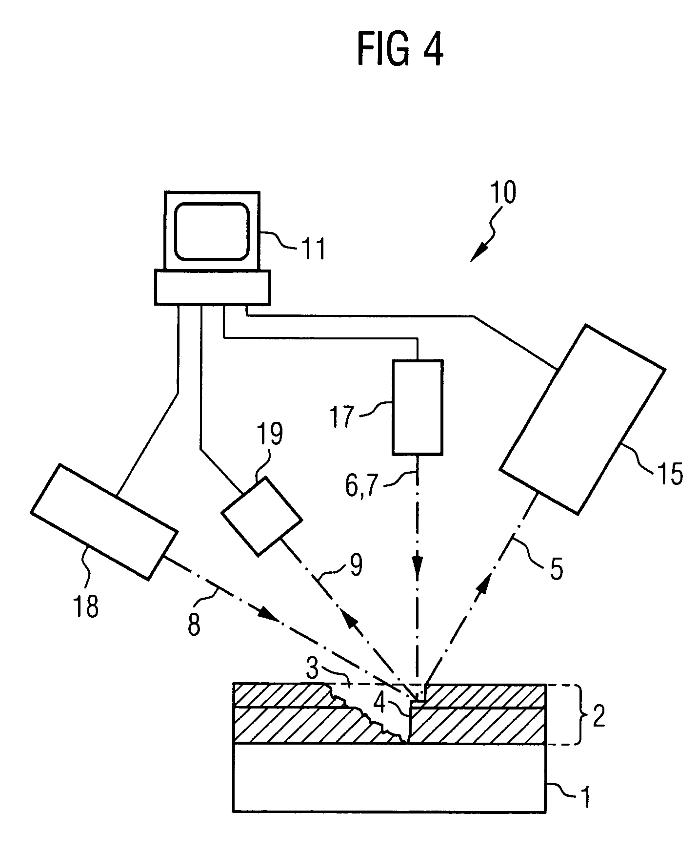
[0029] FIGS. 1 to 3 show schematic lateral sectional illustrations of a detail from a wafer 1 on which a preferred embodiment of a method according to the invention is carried out. The method is used for determining a (depth) profile of a dopant concentration of the wafer 1 in order subsequently to supervise doping processes carried out on the wafer 1. On account of the doping processes, the wafer 1 has a doped layer 2 extending into the depth from the surface, which doped layer is divided for example into two partial regions with different dopant concentrations that are arranged one above the other. The partial regions of the layer 2 are identified by different hatching in FIGS. 1 to 3.

[0030] At the beginning of the method, as shown in FIG. 1, a preferably wedge- or V-shaped cutout 3 is produced in the layer 2 of the wafer 1 with the aid of a focused ion beam 6 directed onto the surface of the wafer 1 or of the layer 2 at an oblique angle of incidence. The cutout 3 has a sidewall ...


PUM


Abstract

The present invention relates to a method for the depth-resolved characterization of a layer of a carrier. This involves firstly producing a cutout in the layer of the carrier with a sidewall and subsequently removing carrier material adjoining the sidewall with the aid of an ion beam. During the removal process, images of the sidewall are recorded and material compositions of the removed carrier material are determined as well. A depth-resolved characterization of the layer of the carrier is carried out on the basis of a correlation of the determined material compositions of the removed carrier material with the recorded images of the sidewall, layer depths being assigned to the material compositions of the removed carrier material with the aid of the images of the sidewall. The invention furthermore relates to an apparatus for carrying out this method.

Description

CLAIM FOR PRIORITY [0001] This application claims the benefit of priority to German Application No. 10 2004 049 518.1 which was filed in the German language on Oct. 11, 2004, the contents of which are hereby incorporated by reference. TECHNICAL FIELD OF THE INVENTION [0002] The present invention relates to an apparatus and method for the depth-resolved characterization of a layer of a carrier. BACKGROUND OF THE INVENTION [0003] Microelectronic semiconductor components with integrated circuits nowadays form the basis for all kinds of electronic applications. These components comprise a complex arrangement of electronic structures which are connected up to one another in a plurality of planes arranged one above the other on a carrier substrate referred to as a chip. The joint production of chips on a substrate slice, also referred to as a wafer, is distinguished by a complicated sequence of a multiplicity of different production steps. [0004] One important production step is so-called...

Claims


Application Information

Patent Timeline
IPC IPC(8): G01J5/02
CPCH01L22/12
Inventor BLOESS, HARALDMANTZ, ULRICH
Owner POLARIS INNOVATIONS
Why Eureka
Try Eureka