Ceramic multilayer substrate
- Summary
- Abstract
- Description
- Claims
- Application Information
AI Technical Summary
Benefits of technology
Problems solved by technology
Method used
Image
Examples
first preferred embodiment
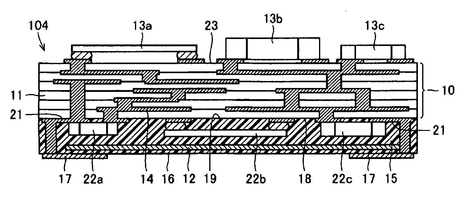
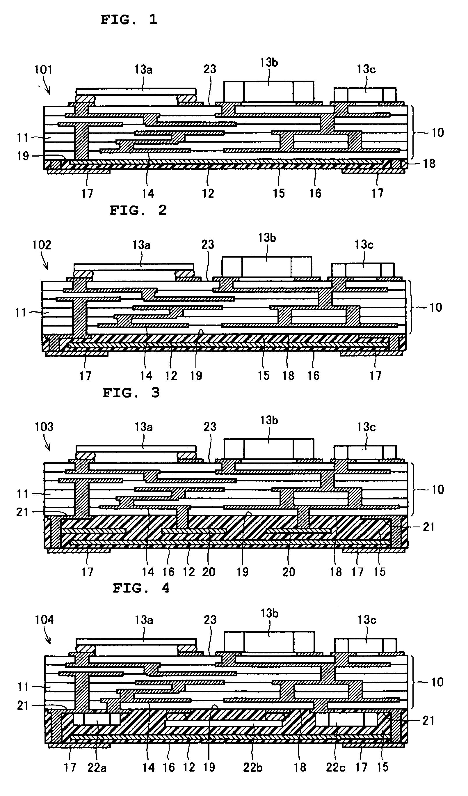
[0033] A ceramic multilayer substrate 101 according to a first preferred embodiment of the present invention will be described with reference to FIG. 1. This ceramic multilayer substrate 101 is provided with a ceramic laminate 10 including a plurality of laminated ceramic layers 11. Internal circuit elements 14 are disposed in the inside of the ceramic laminate 10. The internal circuit elements 14 include via hole conductors extending in ceramic layers 11 in a direction of lamination and in-plane conductors disposed at interfaces between the ceramic layers 11. The ceramic laminate 10 includes a bottom surface defining a first main surface 18. A ground electrode 12 is arranged so as to cover the first main surface 18 of the ceramic laminate 10. Furthermore, a resin layer 15 is arranged so as to cover the ground electrode 12.
[0034] The resin layer 15 includes a bonding surface 19 in contact with the first main surface 18 and a mounting surface 16 opposite to the bonding surface 19. E...
second preferred embodiment
[0046] A ceramic multilayer substrate 102 according to a second preferred embodiment of the present invention will be described with reference to FIG. 2. In this ceramic multilayer substrate 102, the ground electrode 12 is disposed in the inside of the resin layer 15, and is sandwiched by the resin layer 15 from above and below, so as to prevent contact with the first main surface 18. The configurations of the other portions are similar to those described in the first preferred embodiment.
[0047] In the present preferred embodiment, there is no portion in which the ground electrode 12 and the ceramic layer 11 are in direct contact with each other, and therefore, problems, e.g., cracks resulting from the difference in heat shrinkage between the ground electrode 12 and the ceramic layer 11 are reliably prevented.
[0048] The structure shown in FIG. 2 may be constructed by laminating a plurality of resin sheets to form the resin layer 15, and inserting copper foil between the sheets. Th...
third preferred embodiment
[0049] A ceramic multilayer substrate 103 according to a third preferred embodiment of the present invention will be described with reference to FIG. 3. In this ceramic multilayer substrate 103, the capacitor electrodes 20 are provided in addition to the ground electrode 12 on the surface of an internal layer of the resin layer 15. The capacitor electrodes 20 are electrodes which face the ground electrode 12 from the side opposite to the mounting surface 16 and, thereby, define capacitors in combination with the ground electrode 12. These capacitors are electrically connected to the internal circuit elements 14 to define predetermined circuits. The configurations of the other portions are similar to those described in the second preferred embodiment. The capacitor electrodes 20 may be provided at the interface between the ceramic laminate 10 and the resin layer 15.
[0050] In this ceramic multilayer substrate 103, the capacitors are defined by the capacitor electrodes 20 and the grou...
PUM
| Property | Measurement | Unit |
|---|---|---|
| Electrical conductor | aaaaa | aaaaa |
Abstract
Description
Claims
Application Information
 - R&D Engineer
- R&D Manager
- IP Professional
- Industry Leading Data Capabilities
- Powerful AI technology
- Patent DNA Extraction
Browse by: Latest US Patents, China's latest patents, Technical Efficacy Thesaurus, Application Domain, Technology Topic, Popular Technical Reports.
© 2024 PatSnap. All rights reserved.Legal|Privacy policy|Modern Slavery Act Transparency Statement|Sitemap|About US| Contact US: help@patsnap.com


