Display device

a technology of display panel and display image, which is applied in the direction of static indicating device, optics, instruments, etc., can solve the problems of reducing the effective display area, the on-screen display image is difficult to be seen at dark places, and the display panel fails to offer eye-friendly display performance with enough contrast properties, etc., to achieve the effect of improving light-emitting display characteristics and prolonging the life of reflective display characteristics

Inactive Publication Date: 2006-04-20
KK TOSHIBA
View PDF4 Cites 51 Cited by
  • Summary
  • Abstract
  • Description
  • Claims
  • Application Information

AI Technical Summary

Benefits of technology

[0016] An object of this invention is to provide a display device capable of performing both reflective display and light-emitting display operation

Problems solved by technology

Unfortunately, as for the reflective display, the display panel fails to offer eye-friendly display performances with enough contrast properties.
This reason can be said because it suffers from limitations based on LCD's display principles, such as the use of a polarizer plate(s).
Another reason is that each pixel is subdivided into two areas, one of which is exclusively used for reflective display, and the other of which is for light emission display, resulting in a decrease in effective display area.
However, this ECD panel has the reflective displaying capability only, so its on-screen display images are difficult to be seen at dark places.
This results in a chan

Method used


Image

  • Display device
  • Display device
  • Display device

Examples


example 1

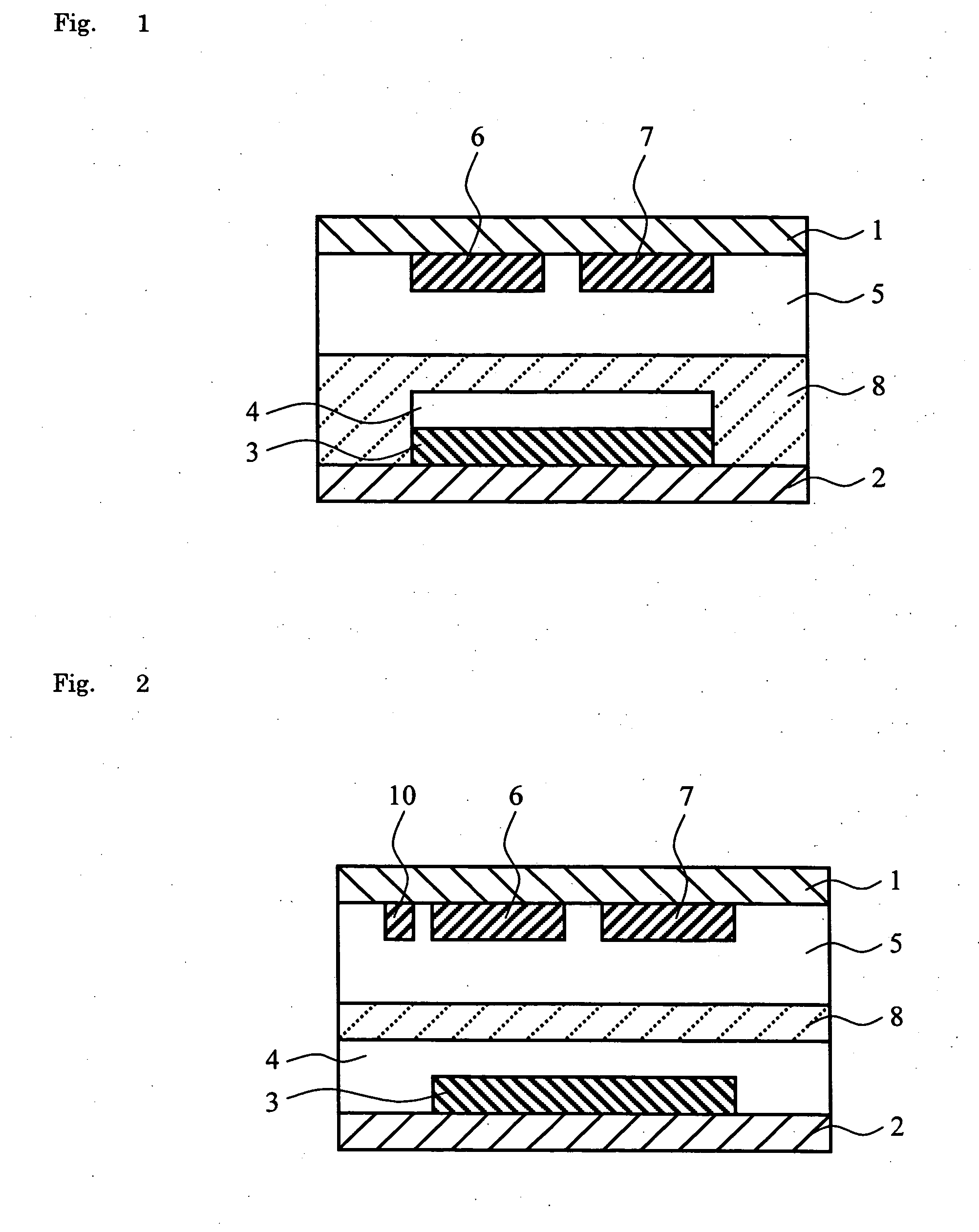
[0078] A square flat display panel with each side of 2.5 inches was prepared in a way which follows. Note here that each pixel was designed to consist of a mono-color electrochemical reactive element having its structure such as shown in FIG. 2. The display panel was formed so that a single pixel measures 100 μm in each side.

[0079] Firstly, a glass substrate having a thickness of 1.1 mm was used as the first substrate 1. A thin film of indium tin oxide (ITO) was then formed on the glass substrate by sputter techniques to a thickness of 100 nanometers (nm). Then, the ITO film was patterned, thus forming the first and second electrodes 6-7. An Ag film was formed by sputtering to a thickness of 100 nm, followed by patterning to thereby provide the reference electrode 10 of FIG. 2.

[0080] A glass substrate was used as the second substrate 2. An ITO film was formed thereon to a thickness of 100 nm and then patterned to form the third electrode 3. The second substrate 2 with the third el...

example 2

[0088] A display device was formed in a similar way to that of Example 1, except that the third layer 8 and ECL layer 5 were formed in a different way which follows.

[0089] Polyethyleneoxide (average molecular weight of 6000) and 0.04 mol of LiCF3SO3 per its ionic dissociation group (ethyleneoxide) were blended in an acetonitrile and then stirred, thus providing a solution. This solution was then coated by a die coater onto the EC layer 4 while controlling its thickness to 6 μm. A coated film was dried at 80° C., thereby preparing the third layer 8.

[0090] In addition, for the cell, 5% of poly[9,9-bis(3,6-dioxaheptyl)-fluorene-2,7-diyl] (BDOH—PF) was dissolved in orthodichlorobenzene, followed by injection into this cell. Thus the ECL layer 5 was obtained.

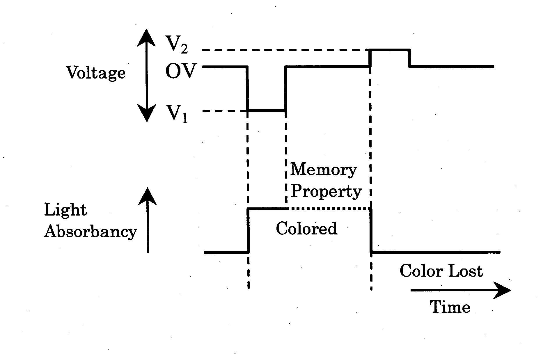
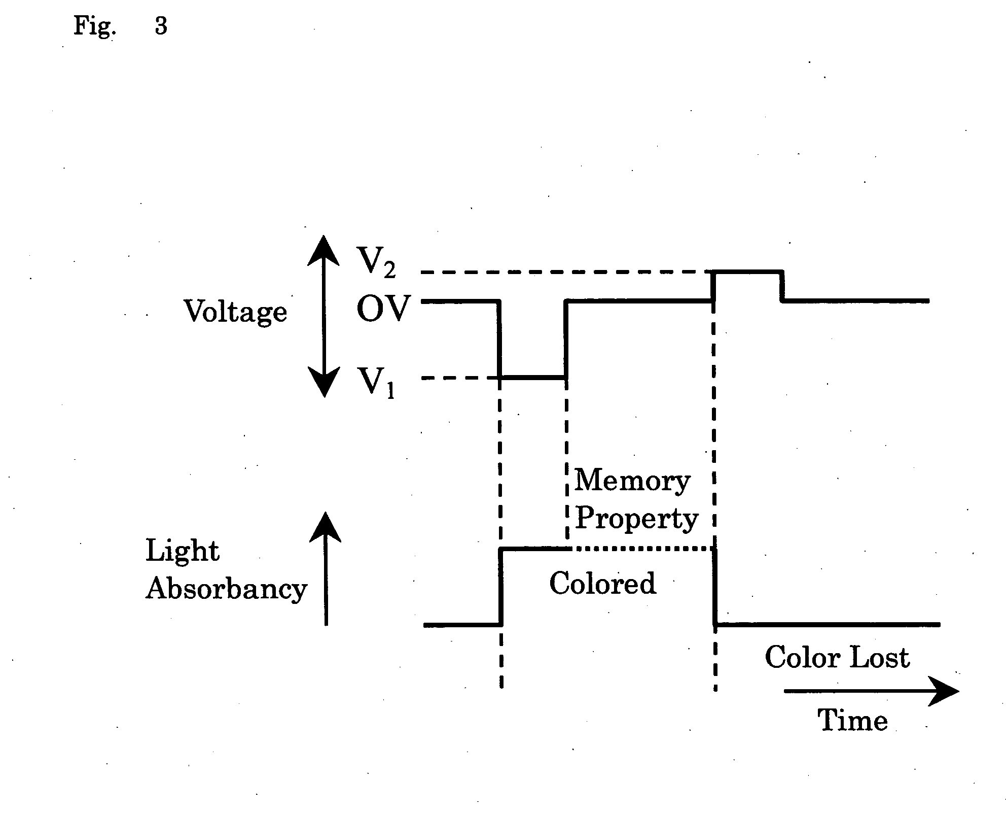
[0091] In this cell structure with the first or second electrode 6, 7 and the third layer 8 being spaced apart from each other by a distance of 2 μm, voltage application was done so that the third electrode 3 is positive or negati...

example 3

[0093] A display device was formed in a similar way to that of Example 2, except that the third layer 8 was prepared in a way which follows.

[0094] A 10 μm-thick nonwoven fabric made of polyethylene (PE) was prepared. Then, divinylbenzene and lithium (Li) styrenesulfonate were impregnated in the fabric and then heated for thermal polymerization, resulting in formation of a thin-film of 10 μm thick with a copolymer of sulfonyl group-owning styrene and divinylbenzene being impregnated in the nonwoven fabric. This was cut into a portion having the cell size, which was then put on the EC layer.

[0095] In this cell with the first or second electrode 6, 7 and the third layer 8 being spaced apart by a distance of 2 μm, voltage application was done so that the third electrode 3 is positive or negative relative to the reference electrode 10 while setting the first and second electrodes 6-7 to the same potential level. Successful achievement of coloring and color-disappearing was demonstrated...


PUM


Abstract

A display device with both light-emitting and reflective display capabilities is disclosed. This device includes first and second electrodes provided on a first substrate, a second substrate provided to be spaced apart from and oppose the first substrate, a third electrode provided on the second substrate, a first layer which is provided between the first and second substrates on the first substrate side and which contains a light emissive material that emits light through electrochemical oxidation or reduction, a second layer which is provided between the first and second substrates on the second substrate side and which includes a coloring material that changes in color due to electrochemical oxidation or reduction, and a third layer between the first and second layers. The third layer is an electrolytic layer having non-transmissivity or transmission retardancy against the light emissive material or its oxidation or reduction species.

Description

CROSS-REFERENCE TO RELATED APPLICATION [0001] This application is based upon and claims the benefit of priority from the prior Japanese Patent Application No. 2004-301402, filed on Oct. 15, 2004, the entire contents of which are incorporated herein by reference. BACKGROUND OF THE INVENTION [0002] 1. Field of the Invention [0003] The present invention relates generally to display devices using a material that exhibits electrogenerated chemiluminescence, also known as electrochemiluminescence (ECL), and a material exhibiting electrochromic (EC) phenomena. [0004] 2. Related Art [0005] Half-transmissive liquid crystal display (LCD) devices offer both reflective displaying capability and light-emitting displaying capability, and are thus widely used as display panels of indoor / outdoor-use handheld electronic equipment, such as mobile cellular phones. Prior known half-transmissive LCD panels are designed so that a reflector layer with a convexo-concave surface is provided at part of a pic...

Claims


Application Information

Patent Timeline
IPC IPC(8): G09G5/36
CPCG02F1/1525G02F1/155G02F1/157G09G3/3433G09G2300/023G09G2310/06
Inventor MIZUNO, YUKITAMIENOMOTO, SHINTAROIKEDA, NARU
Owner KK TOSHIBA
Why Eureka
Try Eureka