Filter control method, signal processing circuit and integrated circuit for wireless receiver

a filter and signal processing circuit technology, applied in electrical equipment, digital transmission, transmission monitoring, etc., can solve the problems of modulated data, deterioration of modulated data, and increase the bit error rate, so as to satisfy the sensitivity and interference wave resistance of the receiver and the effect of low cos

Inactive Publication Date: 2006-04-20
RENESAS ELECTRONICS CORP
View PDF9 Cites 35 Cited by
  • Summary
  • Abstract
  • Description
  • Claims
  • Application Information

AI Technical Summary

Benefits of technology

[0010] The object of the present invention is to provide a method and an apparatus for controlling a filter in a wireless receiver which can solve the above-mentioned problem, can be manufactured at low cost, and can satisfy good receiver sensitivity and interference wave resistance.

Problems solved by technology

As shown FIG. 12, not only the interference wave components but also the desired wave components are largely suppressed because the passband is narrow, which consequently causes a distortion in modulated data to thereby increase the bit error rates.
In the case of such a fixed filter, even when a filtering function is not essentially required because of little interference wave components, a signal passes through the filter with a narrow passband, thus deteriorating the modulated data due to the above-mentioned passband limitation.
As described above, there is a problem that the use of the fixed filter with a narrow passband causes deterioration in the desired wave signal and decrease in receiver sensitivity.

Method used


Image

  • Filter control method, signal processing circuit and integrated circuit for wireless receiver
  • Filter control method, signal processing circuit and integrated circuit for wireless receiver
  • Filter control method, signal processing circuit and integrated circuit for wireless receiver

Examples


first embodiment

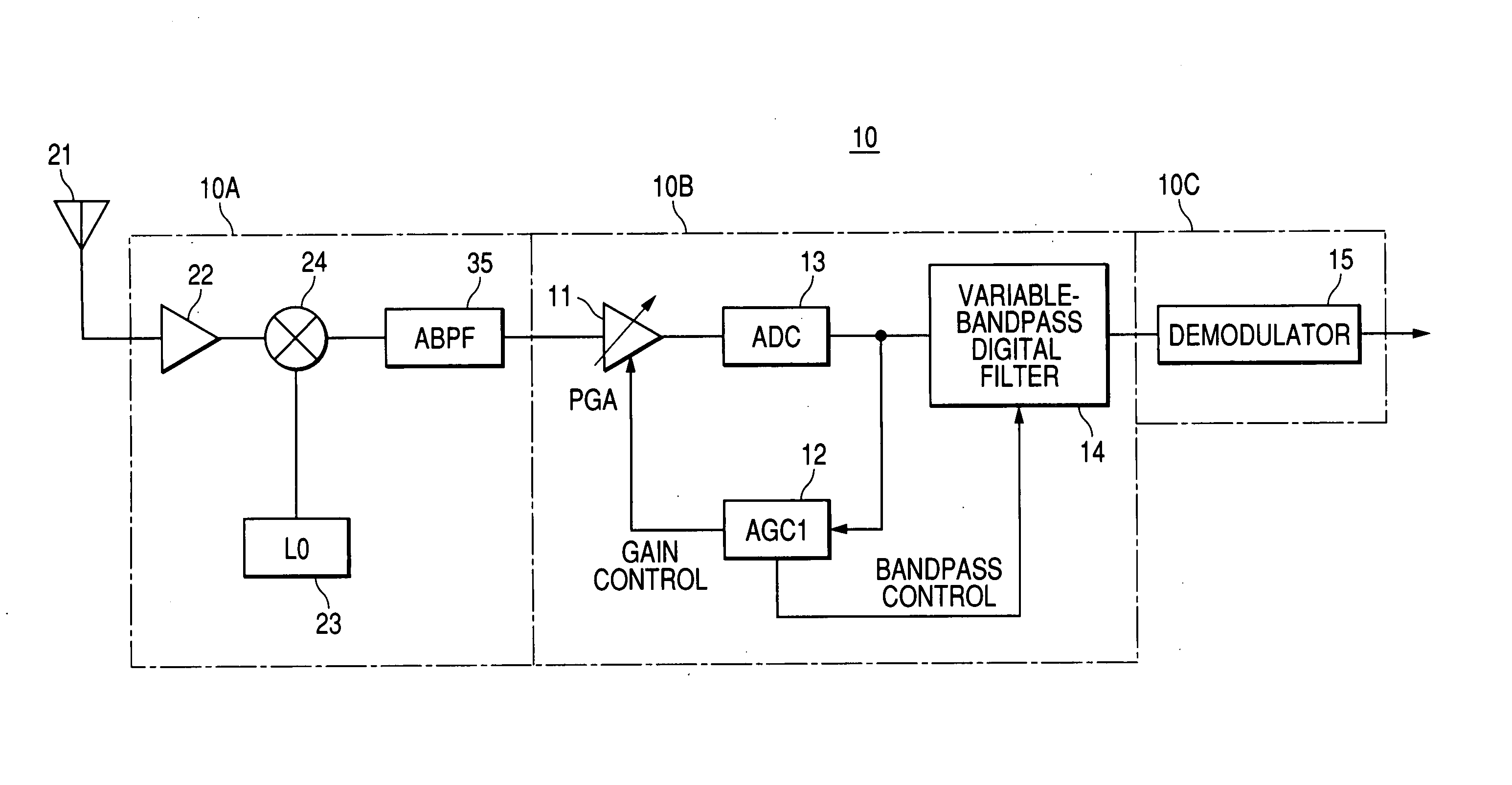
[0030]FIG. 1 is a block diagram showing a circuit configuration of a wireless receiver having a Low-IF architecture according to the present invention. This embodiment exemplifies a case in which an IC for wireless receiver having a variable-bandpass filter configured as a digital filter is applied to a transceiver. A circuit unit of the wireless receiver comprises a high-frequency signal processing unit 1A, a low-frequency signal processing unit 10B and a demodulation unit 10C. A high-frequency signal received by an antenna 21 is amplified by a low noise amplifier 22 in the high-frequency signal processing unit 10A, and then mixed with a reference wave from a local oscillator circuit (LO) 23 by a mixer 24 so as to be converted to a low-frequency signal. The low-frequency signal is supplied to a programmable gain amplifier (PGA) 11 in the low-frequency signal processing unit 10B through an analog filter (ABPF) 35.

[0031] A gain is set to the PGA 11 by a gain control signal from an au...

second embodiment

[0051] Next, the present invention will be described with reference to FIGS. 7 to 10. In FIG. 7, a circuit unit of a wireless receiver comprises a high-frequency signal processing unit 10A, a low-frequency signal processing unit 10B and a demodulation unit 10C. PGAs 81, 83 of the low-frequency signal processing unit 10B amplify the input signal by a gain that is set by an AGC2 85. A variable-bandpass analog filter 82 serves to suppress interference wave components included in the output signal from the PGA1 81, and the passband or the amount of suppression is controlled by the AGC2 85. Further, an ADC 84 converts the output signal from the PGA2 83 into a binary value.

[0052] Here, the PGA1 81 is installed in order to reduce a relatively large noise that is generated by the variable-bandpass analog filter 82. The PGA2 83 serves to adjust the amplitude level of the signal so as to be equal to the input dynamic range of the ADC 84.

[0053] The signal output from the PGA2 83 is converted ...


PUM


Abstract

A conventional method of controlling the passband of a filter involves an increase in cost for a chip due to a large area of a detection circuit for determining the level of an interference wave. The present invention utilizes a result obtained by detecting the amplitude level of a signal with an automatic gain control circuit to appropriately control the passband of a filter. The amplitude level of all the signals including a desired wave and an interference wave is detected by utilizing the automatic gain control circuit to thereby control the passband of a filter on the basis of the result.

Description

CLAIM OF PRIORITY [0001] The present application claims priority from Japanese application JP 2004-303887 filed on Oct. 19, 2004, the content of which is hereby incorporated by reference into this application. FIELD OF THE INVENTION [0002] The present invention relates to a method and an apparatus for controlling the passband of a filter in a receiver, and particularly to a method and an apparatus for controlling, with a simple structure, the passband of a filter that suppresses an interference wave in accordance with an incoming signal in an integrated circuit (hereinafter, abbreviated as IC) for a wireless receiver. BACKGROUND OF THE INVENTION [0003] In a conventional technique, a wireless receiver employs a configuration in which two bandpass filters are utilized in order to detect an adjacent interference wave (for example, see Japanese Patent Laid-Open No. 2004-72576). SUMMARY OF THE INVENTION [0004]FIG. 11 shows a general configuration of a wireless receiver having a Low-IF ar...

Claims


Application Information

Patent Timeline
Patent Type & Authority Applications(United States)
IPC IPC(8): H04B1/06H04L27/08H04B1/10H04B1/7093H04B1/713H04B1/715
CPCH04B1/1027
Inventor OSHIMA, TAKASHIKOKUBO, MASARU
Owner RENESAS ELECTRONICS CORP
Why Eureka
Try Eureka