Wire structure, semiconductor device, MRAM, and manufacturing method of semiconductor device

a manufacturing method and wire structure technology, applied in the field of wire structure, semiconductor devices, mrams, and manufacturing methods of semiconductor devices, can solve the problems that the value of the current that is allowed to flow through these downsized copper wires cannot help being made smaller, and achieve the effect of suppressing fusion cutting of wires, reducing the resistance of the entire wire, and increasing the current density of curren

Inactive Publication Date: 2006-04-27
RENESAS TECH CORP
View PDF6 Cites 64 Cited by
  • Summary
  • Abstract
  • Description
  • Claims
  • Application Information

AI Technical Summary

Benefits of technology

[0009] A current having a large current density can be made to flow through this wire. Accordingly, even in the case where the wire is downsized, it is not necessary to reduce the amount of current that flows through it.
[0021] The carbon nanotubes can be grown in a direction comprising a direction component in which the trench extends. Accordingly, the resistance of the entire wire can be reduced. Furthermore, effects such as an increase in the current density of a current that flows through the wire, suppression of fusion cutting of the wire, and restriction of the occurrence of migration can be attained.

Problems solved by technology

Thus, the value of the current that is allowed to flow through these downsized copper wires cannot help being made smaller, taking into consideration the migration phenomenon and the like that occurs in copper wires.

Method used


Image

  • Wire structure, semiconductor device, MRAM, and manufacturing method of semiconductor device
  • Wire structure, semiconductor device, MRAM, and manufacturing method of semiconductor device
  • Wire structure, semiconductor device, MRAM, and manufacturing method of semiconductor device

Examples


first embodiment

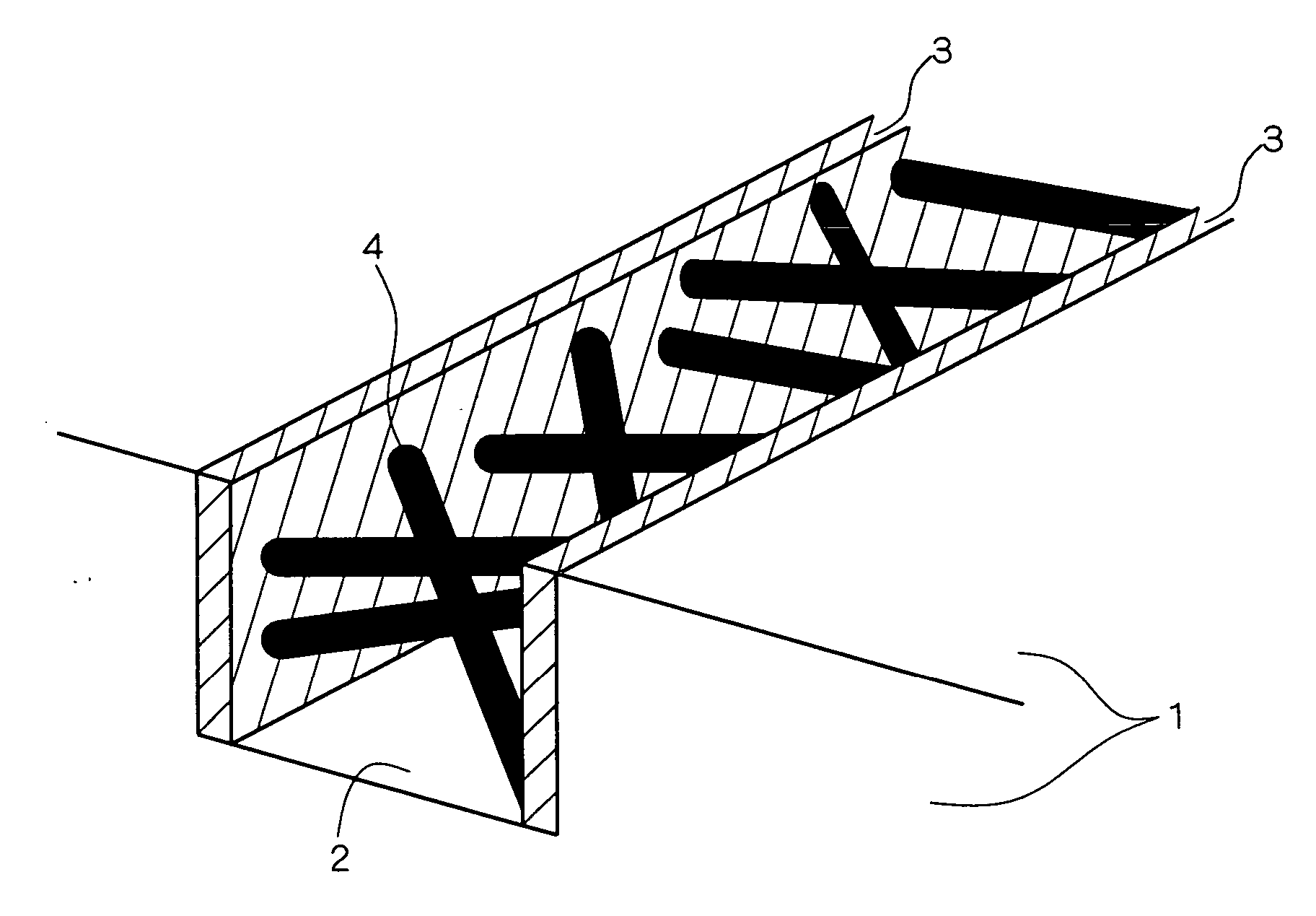
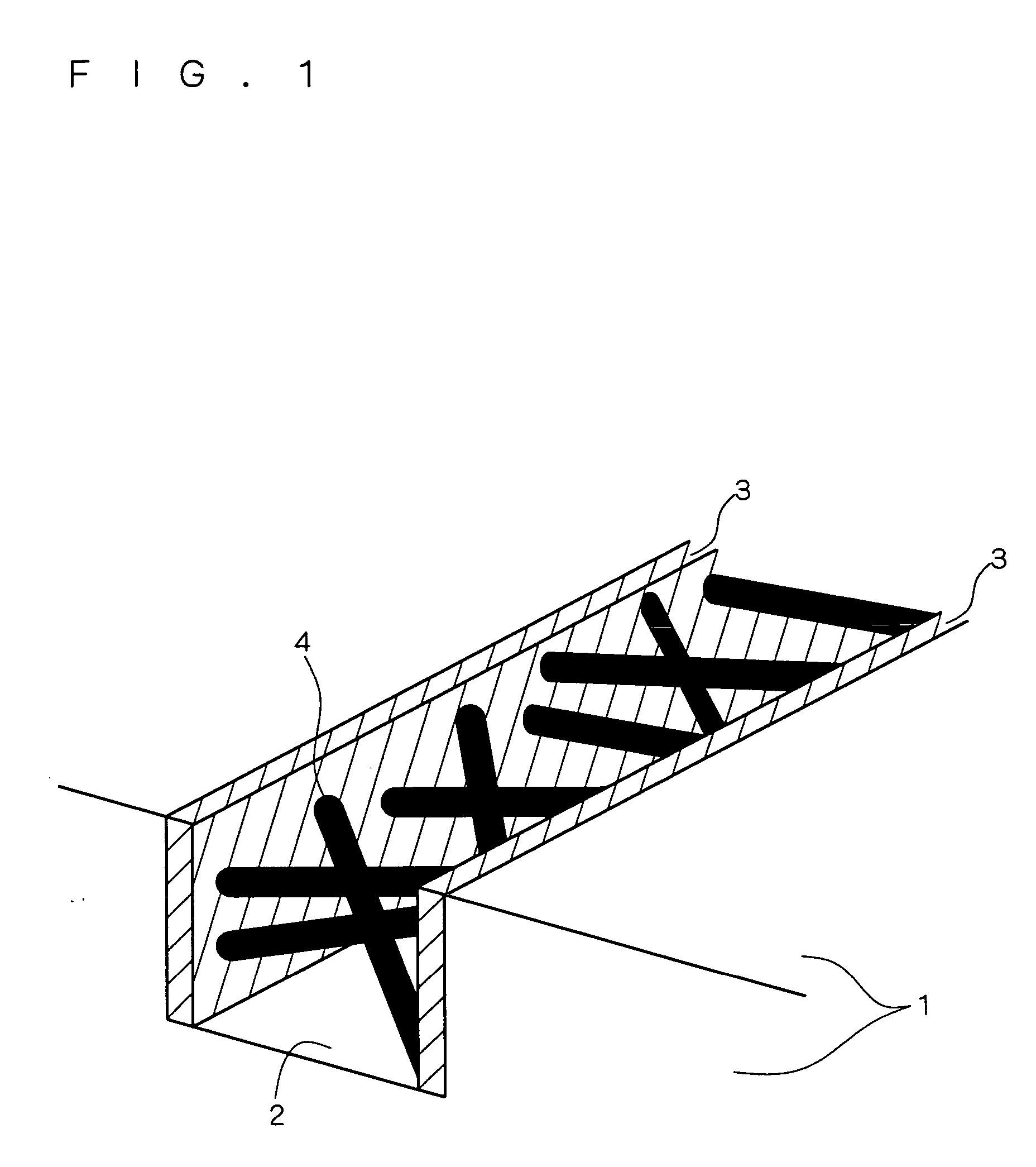
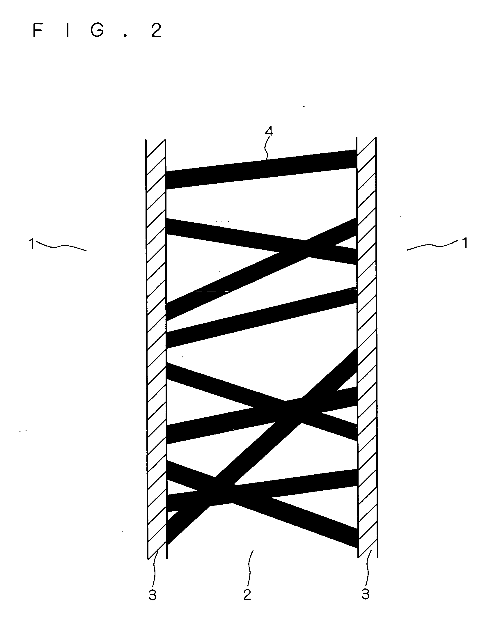
[0064]FIG. 1 is an enlarged perspective view showing a wire structure according to a first embodiment. In addition, FIG. 2 is a top view showing the wire structure according to this embodiment. In addition, FIG. 3 is a perspective cross-sectional view showing the wire structure according to this embodiment.

[0065] Here, FIGS. 1, 2 and 3 depict only several carbon nanotubes 4, for the purpose of simplifying the drawings. Actually, however, the carbon nanotubes 4 exist in a trench 2 more densely than in the figures. In addition, the directions in which the carbon nanotubes 4 grow are more complex actually, and carbon nanotubes grow in random directions.

[0066] As shown in FIGS. 1 to 3, an interlayer insulating film 1 is formed on a semiconductor substrate 10. A trench 2 of which the cross section is approximately rectangular is formed in the surface of the interlayer insulating film 1. In addition, conductive catalyst films 3 are formed on the surface on both sides of the trench 2.

[0...

second embodiment

[0088]FIG. 8 is a perspective cross-sectional view showing a wire structure according to a second embodiment.

[0089] As shown in FIG. 8, in the wire structure according to this embodiment, the inside of a trench 2 in which carbon nanotubes 4 are formed is filled in with a conductor (for example, copper) 6. Furthermore, a barrier film 5 is formed in order to prevent the diffusion of this conductor 6 into an interlayer insulating film 1.

[0090] This barrier film 5 is formed on the inner surfaces of the sides and the bottom of the trench 2. Here, the barrier film 5 is formed between the interlayer insulating film 1 and the conductor 6 on the bottom and between catalyst films 3 and the interlayer insulating film 1 on the sides of the trench 2. This is because the carbon nanotubes 4 are not prevented from growing on the catalyst films 3.

[0091] The other configurations are the same as those of the wire structure according to the first embodiment.

[0092] Next, a manufacturing method of th...

third embodiment

[0112]FIG. 14 is a perspective cross-sectional view showing a wire structure according to a third embodiment.

[0113] As shown in FIG. 14, a catalyst film 3 having conductivity is also formed on the bottom of the trench 2 in the wire structure according to this embodiment. Accordingly, as shown in FIG. 14, carbon nanotubes 4 also grow on the catalyst film 3 that exists on the bottom of the trench 2.

[0114] The other configurations are the same as those in the wire structure according to the first embodiment.

[0115] Next, a manufacturing method of the wire structure according to this embodiment is concretely described with reference to the cross-sectional views showing the steps thereof.

[0116] First, a structure as shown in FIG. 6 is prepared.

[0117] Next, as shown in FIG. 15, a resist 11 is applied to the catalyst film 3 so as to fill in the trench 2.

[0118] Next, etch back is carried out on the resist 11. As a result of this, as shown in FIG. 16, resist 11 remains only on the botto...


PUM


Abstract

The present invention provides a wire structure where reduction in the amount of current that can be made to flow through the wire can be suppressed (a current comprising a large current density can be made to flow), even in the case where the wire is downsized. A wire structure according to the present invention is provided in an insulating film formed on a base. Here, a trench is formed in the surface of the insulating film. In addition, a plurality of carbon nanotubes are included in this trench. That is, the wire structure according to the present invention includes at least a plurality of carbon nanotubes.

Description

BACKGROUND OF THE INVENTION [0001] 1. Field of the Invention [0002] The present invention relates to a wire structure, a semiconductor device, an MRAM, and a manufacturing method of a semiconductor device. In particular, the present invention relates to a wire structure that includes carbon nanotubes, a semiconductor device, an MRAM, and a manufacturing method of a semiconductor device. [0003] 2. Description of the Background Art [0004] Conventional semiconductor devices having a copper wire structure formed in accordance with a Damascene method have existed conventionally (see “Research Report of Trends in Technologies Filed as Patent Applications in Fiscal Year 2003, Multilayer Wire Technologies of LSI (Abridged Version), March 2004, p. 3, FIGS. 1 and 2,” by Japan Patent Office). [0005] Here, in the case where a current of which the current density is about 107 A / cm2 flows through a copper wire, this copper wire is fused and cut. In addition, in the case where a current of which t...

Claims


Application Information

Patent Timeline
Patent Type & Authority Applications(United States)
IPC IPC(8): H01L29/94
CPCB82Y10/00G11C13/025G11C2213/81H01L21/2885H01L21/76843H01L21/76844H01L21/76846H01L21/76847H01L21/76865H01L21/76868H01L21/76876H01L21/76877H01L21/76879H01L23/53276H01L27/228H01L51/0048H01L51/0052H01L2221/1094H01L2924/0002H01L2924/00H10B61/22H10K85/221H10K85/615
Inventor EIMORI, TAKAHISA
Owner RENESAS TECH CORP
Why Eureka
Try Eureka