Semiconductor device and manufacturing method thereof

a technology of semiconductors and semiconductors, applied in the direction of vacuum evaporation coatings, transistors, coatings, etc., can solve the problems of increasing power consumption and inability to apply siosub>2 /sub>

Active Publication Date: 2006-04-27
KIOXIA CORP
View PDF8 Cites 24 Cited by
  • Summary
  • Abstract
  • Description
  • Claims
  • Application Information

AI Technical Summary

Benefits of technology

[0018] forming an oxide film containing at least one selected from the group consisting of Zr, Hf, Ti and a lanthanoid series metal as a gate insulati

Problems solved by technology

In a case of SiO2, leakage current due to direct tunnel current cannot be restrained in an area of this film thickness, and

Method used


Image

  • Semiconductor device and manufacturing method thereof
  • Semiconductor device and manufacturing method thereof
  • Semiconductor device and manufacturing method thereof

Examples


first embodiment

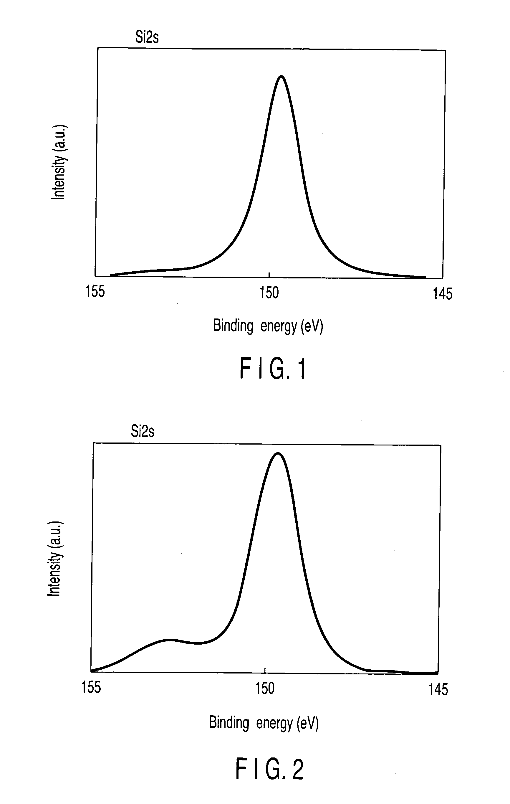
[0038] In a first embodiment, an example will be described wherein an LaAlO gate insulating film is deposited by a laser ablation method.

[0039]FIG. 1 shows an Si2s photoelectron spectrum in an LaAlO film which is formed at a thickness of 5 nm at a room temperature in an atmosphere under an oxygen partial pressure of 5×10⁻⁵ Pa by the laser ablation method using an LaAlO3 single-crystal substrate as a target, on an n-type silicon (100) substrate in which a native oxide film has been removed by dipping diluted HF solution. A strong peak in the vicinity of 150 eV is attributed to a Si substrate. When Si constituting the substrate causes a reaction and a low-dielectric-constant interfacial layer is generated, a peak resulting from a Si oxide is observed in the vicinity of 153 eV, but such a peak is not observed in FIG. 1, and it is thus understood that the low-dielectric-constant interfacial layer is not generated at a room temperature under an oxygen partial pressure of 5×10⁻⁵ Pa.

[004...

second embodiment

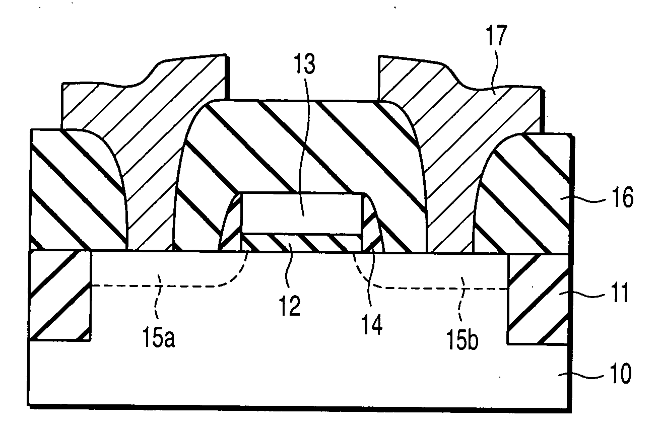
[0057]FIG. 12 is a sectional view showing an element structure of a semiconductor device (MOS transistor) according to a second embodiment of the present invention.

[0058] Reference numeral 10 in FIG. 12 denotes an n-type Si substrate in a plane direction (100), and an element formation area of this substrate 10 is separated by an isolation insulating film 11. A poly-Si gate electrode 13 is formed on the element formation area of the substrate 10 via a gate insulating film 12 including LaAlO. A side wall insulating film 14 comprising a Si nitride film is formed on a side surface of the gate electrode 13, and source / drain regions 15a, 15b comprising p-type diffused layers are formed on a surface of the substrate with the gate electrode 13 in between.

[0059] An interlayer insulating film 16 comprising a silicon oxide film is formed on the substrate 10 where the MOS transistor as described above is formed. Further, a contact hole is formed in the interlayer insulating film to contact t...


PUM

PropertyMeasurementUnit
Temperatureaaaaaaaaaa
Pressureaaaaaaaaaa

Abstract

A semiconductor device includes a Si substrate, a gate insulating film formed on the Si substrate, the gate insulating film being formed of an oxide film containing at least one selected from the group of Zr, Hf, Ti and a lanthanoid series metal, and having a single local minimal value on a high binding energy side of an inflection point in first differentiation of an O1s photoelectron spectrum, and a gate electrode formed on the gate insulating film.

Description

CROSS-REFERENCE TO RELATED APPLICATIONS [0001] This application is based upon and claims the benefit of priority from prior Japanese Patent Application No. 2004-307027, filed Oct. 21, 2004, the entire contents of which are incorporated herein by reference. BACKGROUND OF THE INVENTION [0002] 1. Field of the Invention [0003] The present invention relates to a semiconductor device and a manufacturing method thereof, and more particularly relates to a semiconductor device having a high-dielectric-constant gate insulating film and to a manufacturing method thereof. [0004] 2. Description of the Related Art [0005] Development of Si-LSI has been achieved by a size reduction of elements in accordance with a scaling law. According to this scaling law, a gate insulating film in a next-generation MOS-type field effect transistor having a gate length less than 0.1 μm is required to have a film thickness of 1.5 nm or less in terms of an equivalent thickness of SiO2. [0006] In a case of SiO2, leak...

Claims


Application Information

Patent Timeline
IPC IPC(8): H01L29/94H01L29/788
CPCC23C14/08C23C14/28H01L21/28194H01L21/31641H01L21/31645H01L21/31691H01L29/495H01L29/4966H01L29/517H01L21/02175
Inventor SUZUKI, MASAMICHIYAMAGUCHI, TAKESHI
Owner KIOXIA CORP
Why Eureka
Try Eureka