

Ceramic plate for a semiconductor producing/examining device
a technology of producing/examining devices and ceramic plates, applied in the field of ceramic plates, can solve the problems of warp generation at a high temperature range, wafer-putting/holding faces contracting more easily, and achieving the effect of improving the adhesion between heating elements and ceramic substrates
- Summary
- Abstract
- Description
- Claims
- Application Information
AI Technical Summary
Benefits of technology
Problems solved by technology
Method used
Image

Examples
example 1
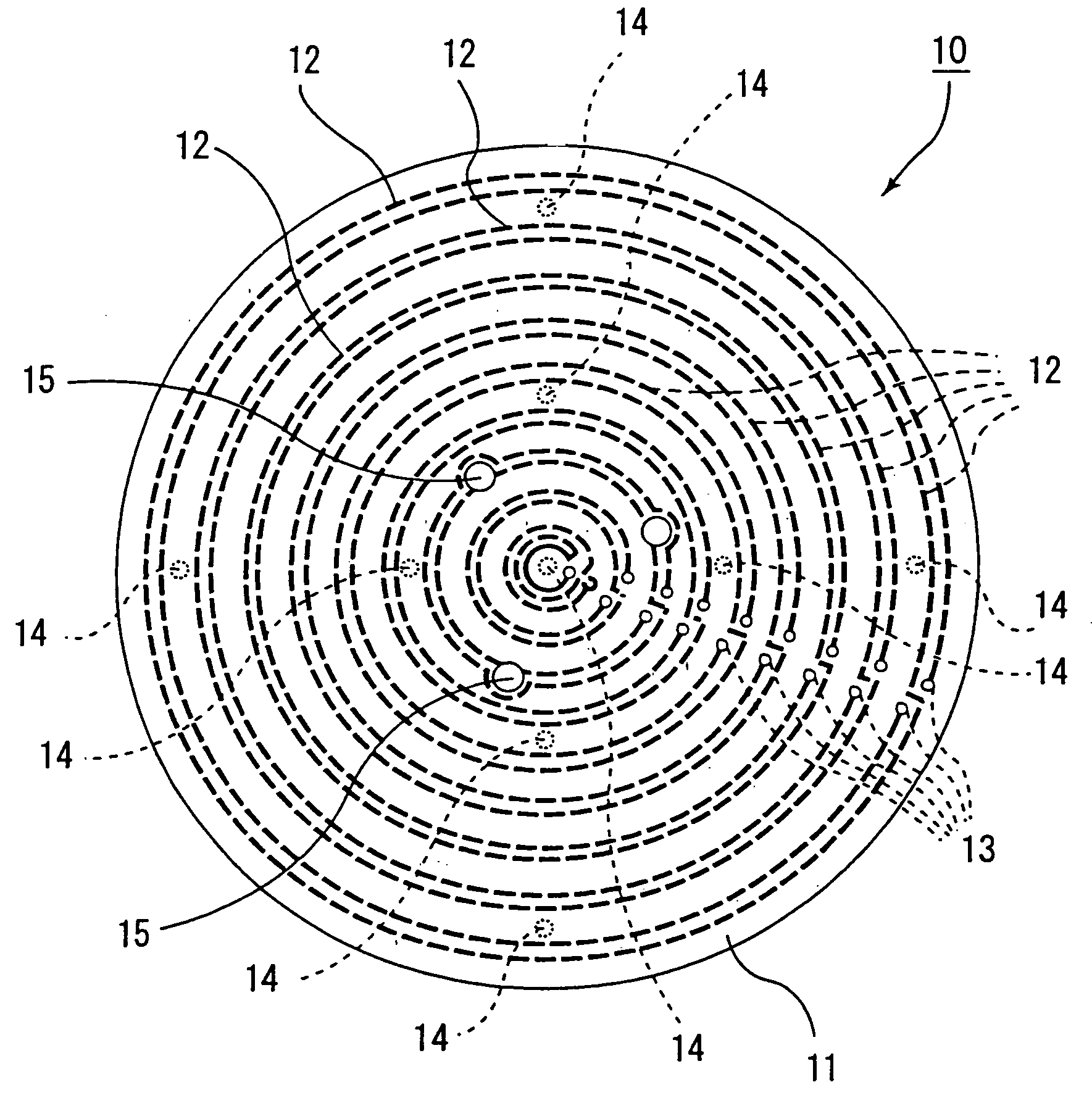
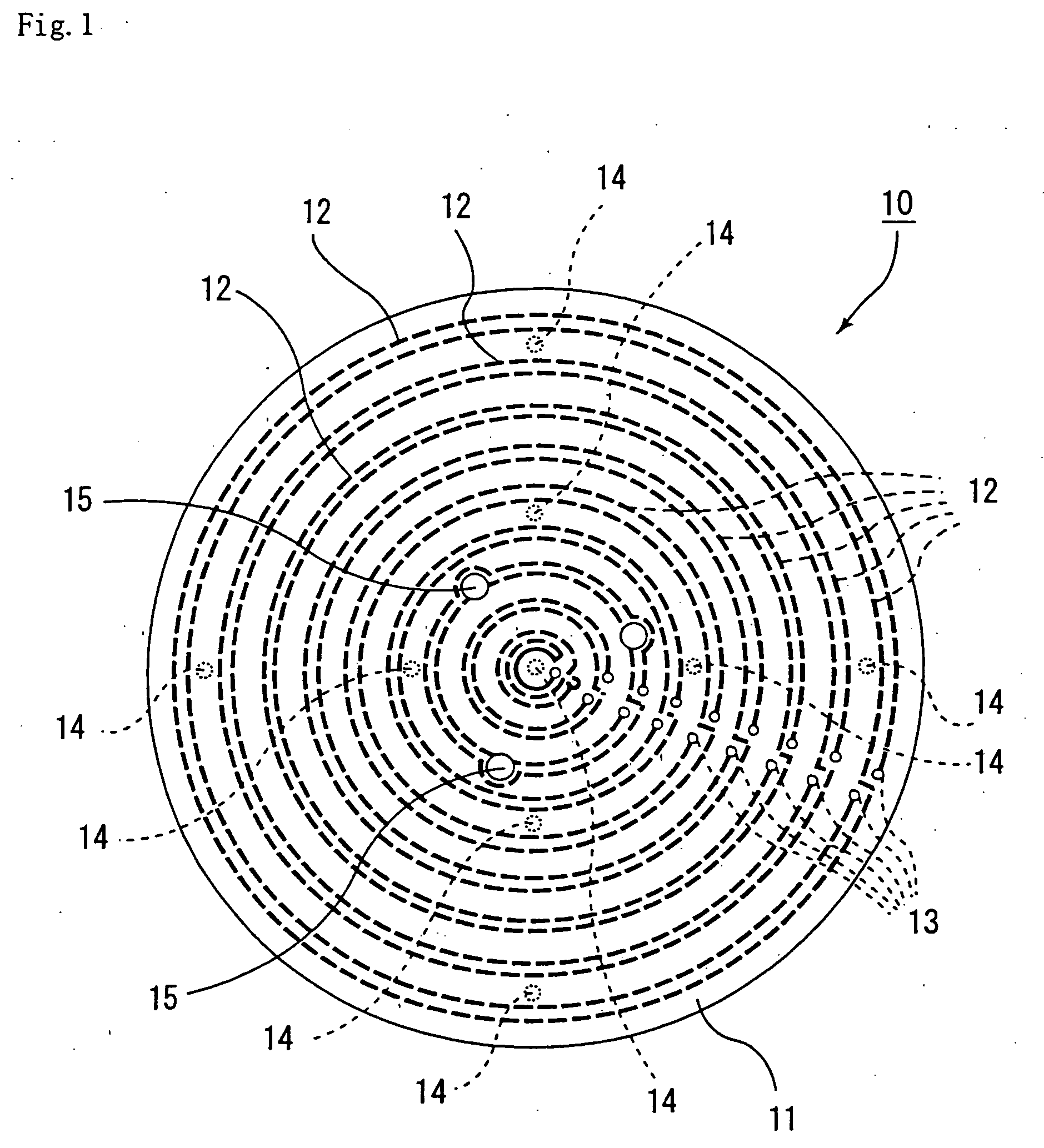
Ceramic Heater
[0130] (1) The following paste was used to conduct formation by a doctor blade method, to obtain green sheets 0.47 mm in thickness: a paste obtained by mixing 100 parts by weight of aluminum nitride powder (made by Tokuyama Corp., average particle diameter: 1.1 μm), 4 parts by weight of yttria (average particle diameter: 0.4 μm), 11.5 parts by weight of an acrylic binder, 0.5 part by weight of a dispersant and 53 parts by weight of alcohol comprising 1-butanol and ethanol.
[0131] (2) Next, this green sheet was dried at 80° C. for 5 hours, and subsequently through holes having a diameter of 1.8 mm, 3.0 mm and 5.0 mm were made by punching. These through holes were portions which would be through holes into which supporting pins for supporting a silicon wafer would be inserted; and portions which would be conductor-filled through holes; and so on.
[0132] (3) The following were mixed to prepare a conductor containing paste A: 100 parts by weight of tungsten carbide partic...
example 2
[0140] (1) A composition made of 100 parts by weight of aluminum nitride powder (average particle diameter: 1.1 μm), 4 parts by weight of yttria (average particle diameter: 0.4 μm), 12 parts by weight of an acrylic binder and an alcohol was subjected to spray-drying to make granular powder.
(2) Next, this granular powder was put into a mold and formed into a flat plate form to obtain a raw formed body (green)
(3) The raw formed body subjected to the working treatment was hot-pressed at 1800° C. and under a pressure of 20 MPa (200 kg / cm2) to obtain a nitride aluminum plate body having a thickness of 3 mm.
[0141] Next, this plate was cut out into a disk having a diameter of 300 mm, and then sandblast treatment of blowing alumina particles having an average particle diameter of 5 μm against both faces thereof was conducted, to make the surface roughness of the wafer-putting / holding face: Rmax=7 μm and that of the opposite face: Rmax=7.5 μm according to JIS B 0601, respectively.
[0142...
example 3
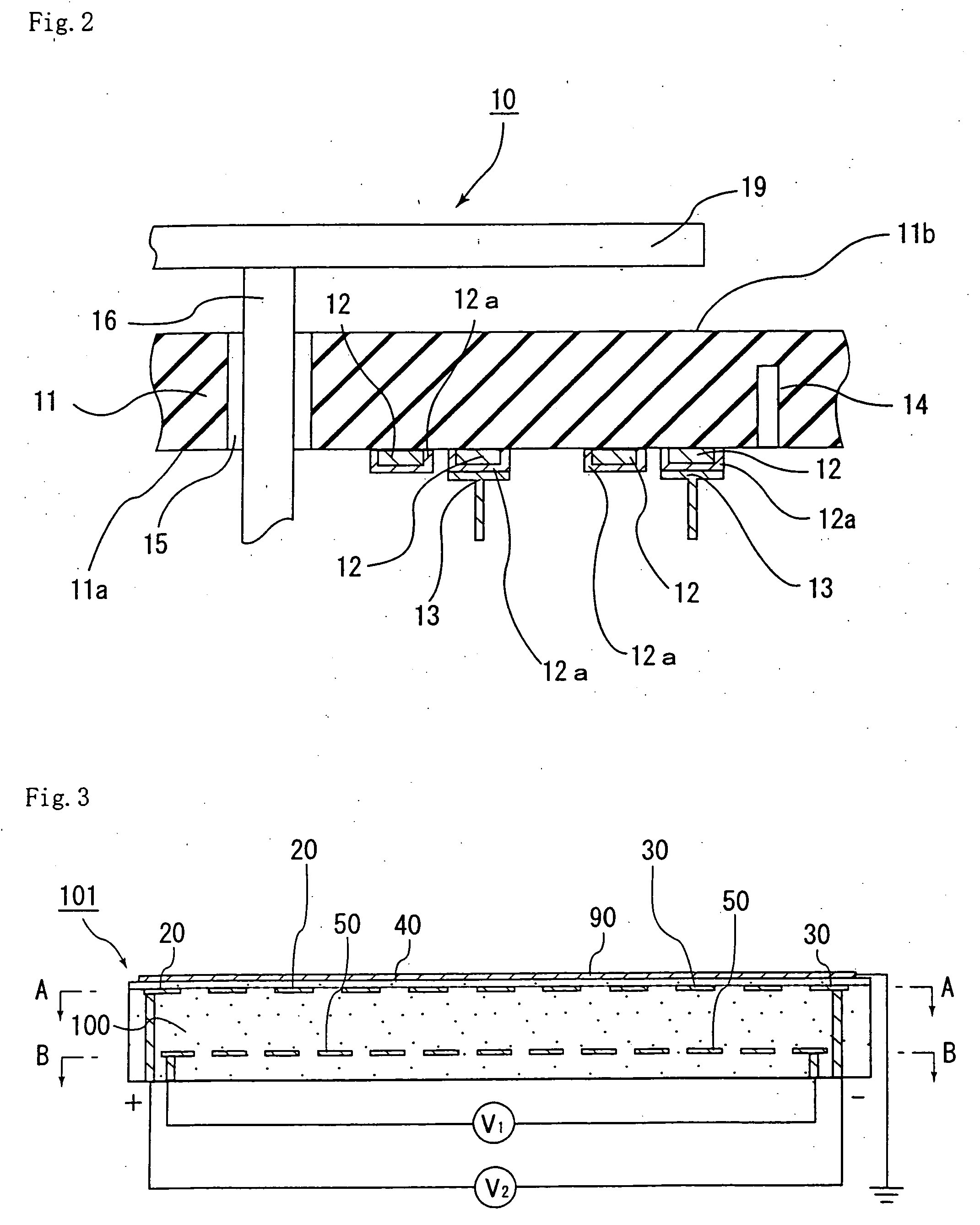
Production of an Electrostatic Chuck (Reference to FIGS. 3 to 5)
[0148] (1) The following paste was used to conduct formation by a doctor blade method, to obtain green sheets 0.47 mm in thickness: a paste obtained by mixing 100 parts by weight of aluminum nitride powder (made by Tokuyama Corp., average particle diameter: 1.1 μm), 4 parts by weight of yttria (average particle diameter: 0.4 μm), 11.5 parts by weight of an acrylic binder, 0.5 part by weight of a dispersant, 0.2 part by weight of saccharose and 53 parts by weight of alcohol comprising 1-butanol and ethanol.
[0149] (2) Next, this green sheet was dried at 80° C. for 5 hours, and subsequently portions which would be through holes into which semiconductor wafer supporting pins having a diameter of 1.8 mm, 3.0 mm and 5.0 mm would be inserted, and portions which would be conductor-filled through holes for attaining connection to external terminals were made.
[0150] (3) The following were mixed to prepare a conductor containin...
PUM
| Property | Measurement | Unit |
|---|---|---|
| Length | aaaaa | aaaaa |
| Fraction | aaaaa | aaaaa |
| Diameter | aaaaa | aaaaa |
Abstract
Description
Claims
Application Information