Photoelectric conversion device

a conversion device and photoelectric technology, applied in the direction of semiconductor/solid-state device manufacturing, semiconductor devices, electrical devices, etc., can solve the problems of reducing the conversion efficiency of thin-film-based photoelectric conversion devices, reducing the output voltage and reducing the conversion efficiency of conventional techniques based on textured transparent electrodes. achieve the effect of improving the conversion efficiency of the photoelectric conversion devi

Inactive Publication Date: 2006-05-04
MITSUBISHI HEAVY IND LTD
View PDF10 Cites 61 Cited by
  • Summary
  • Abstract
  • Description
  • Claims
  • Application Information

AI Technical Summary

Benefits of technology

[0009] Therefore, the present invention addresses providing a novel technique for improving the conversion efficiency of the photoelectric conversion device.

Problems solved by technology

One of the issues of the photoelectric conversion device (for example, a thin film solar cell) using a semiconductor thin film for photoelectric conversion is the improvement in conversion efficiency.
It is inevitable that thin-film-based photoelectric conversion devices experience reduced conversion efficiency compared to that of photoelectric conversion devices integrated in single-crystal semiconductor chips.
The conventional technique based on the textured transparent electrode, however, experiences limitations in the improvement in the conversion efficiency, as disclosed in Yoshiyuki Nasuno et al., “Effects of Substrate Surface Morphology On Microcrystalline Silicon Solar Cells”, Jpn. J. Appl. Phys., the Japan Society of Applied Physics, 1 Apr. 2001, vol.
This difficulty results from the fact that the textured transparent electrode undesirably induces defects within the semiconductor thin film integrated thereon.
Although increasing the light absorption of the semiconductor layer, the irregularities provided on the surface of the transparent electrode undesirably increase the defects within the semiconductor thin film, and cause the reduction in the output voltage of the photoelectric conversion device.
Accordingly, there is a fundamental limitation in achieving improved conversion efficiency through using the textured transparent electrode.

Method used


Image

  • Photoelectric conversion device
  • Photoelectric conversion device
  • Photoelectric conversion device

Examples


Embodiment Construction

[0049] Preferred embodiments of the present invention will be described below in detail with reference to the attached drawings. It should be noted that the same reference numerals denote the same or like components in the drawings.

Device Structure

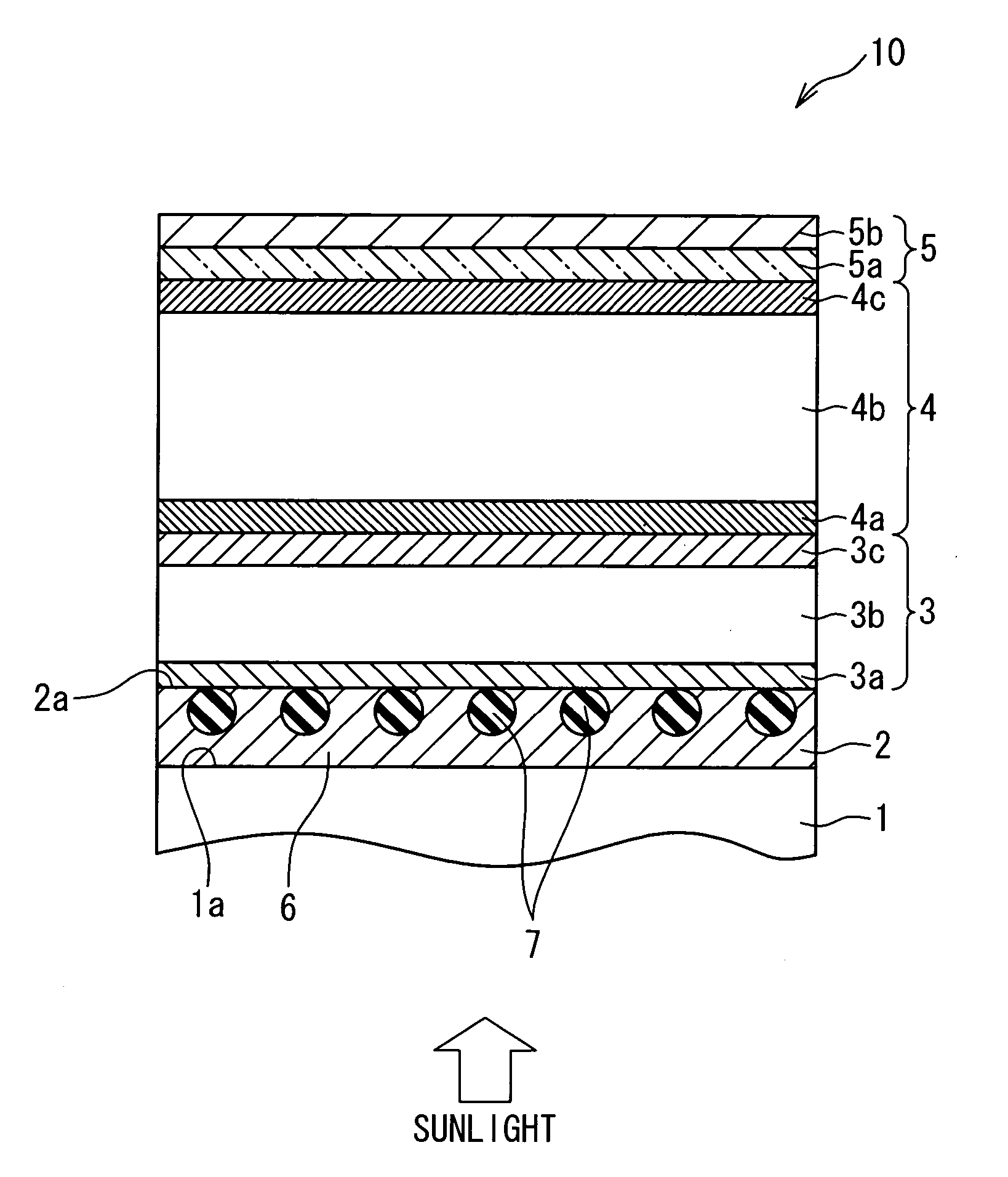
[0050] In one embodiment of the present invention, as shown in FIG. 1, a tandem thin-film solar cell 10 is provided with a glass substrate 1, a lower electrode layer 2, a top cell 3, a bottom cell 4 and an upper electrode layer 5, which are sequentially formed to cover the main surface 1a of the glass substrate 1. The top cell 3 is composed of a p-type amorphous silicon layer 3a, an i-type amorphous silicon layer 3b and an n-type amorphous silicon layer 3c, which are sequentially formed to cover the lower electrode layer 2. The bottom cell 4 is composed of a p-type microcrystalline silicon layer 4a, an i-type microcrystalline silicon layer 4b and an n-type microcrystalline silicon layer 4c, which are sequentially formed to cover the top ...


PUM


Abstract

A photoelectric conversion device is composed of a substrate, a lower electrode layer formed to cover the substrate, and a first semiconductor layer formed on the lower electrode. The lower electrode layer includes a first matrix formed of transparent conductive material, and light scattering granules embedded within the first matrix.

Description

BACKGROUND OF THE INVENTION [0001] 1. Field of the Invention [0002] The present invention relates to photoelectric conversion devices utilizing photoelectric effect to generate power. [0003] 2. Description of the Related Art [0004] One of the issues of the photoelectric conversion device (for example, a thin film solar cell) using a semiconductor thin film for photoelectric conversion is the improvement in conversion efficiency. It is inevitable that thin-film-based photoelectric conversion devices experience reduced conversion efficiency compared to that of photoelectric conversion devices integrated in single-crystal semiconductor chips. The improvement in the conversion efficiency is one of the most important requirements for the commercial use of the thin-film-based photoelectric conversion device. [0005] Providing a textured transparent electrode on a substrate is one of the promising techniques for improving the conversion efficiency, as disclosed in Japanese Patent Gazette No...

Claims


Application Information

Patent Timeline
Patent Type & Authority Applications(United States)
IPC IPC(8): H01L31/00H01L21/00
CPCH01L31/02168H01L31/022425H01L31/022466Y02E10/50
Inventor KOBAYASHI, YASUYUKISAKAI, SATOSHISATAKE, KOJI
Owner MITSUBISHI HEAVY IND LTD
Why Eureka
Try Eureka