LED package with structure and materials for high heat dissipation

a technology of led chips and packaging, applied in the direction of electrical equipment, semiconductor devices, semiconductor/solid-state device details, etc., can solve the problems of limited use of led chips, prior art packages providing inadequate heat dissipation away from led dies, and current led packages cannot handle the high-power density of led chips. achieve the effect of improving heat dissipation, low fracture toughness, and small footprin

Active Publication Date: 2006-05-04
LED ENGIN
View PDF37 Cites 66 Cited by
  • Summary
  • Abstract
  • Description
  • Claims
  • Application Information

AI Technical Summary

Benefits of technology

[0019] The use of a thermally conductive material enhances heat dissipation from the LED to the bottom surface of the package, making it possible to package a high-power LED in a smaller package with a smaller footprint. Because the present disclosure does not require that the thermally conductive material also be electrically conductive, a broader range of thermally conductive materials, particularly ceramics, can be used. In some embodiments, the use of a material with a low fracture toughness (i.e. a low resistance to fracturing), such as AlN ceramic, makes it possible to fabricate multiple LED packages on a single grid that can be later diced into individual LED packages along snap lines. Furthermore, choosing a thermally conductive material that has a coefficient of thermal expansion approximately matching the coefficient of thermal expansion of the LED materials helps to improve the mechanical properties such as reliability of the light emitting device.

Problems solved by technology

Although high-power LED devices have been manufactured, their widespread use has been limited because of a lack of suitable packages for the LEDs.
Current LED packages cannot handle the high-power density of LED chips.
In particular, prior art packages provide inadequate heat dissipation away from the LED dies.
Inadequate heat dissipation limits the minimum size of the package and therefore the density of LEDs per unit area in the device.
Without sufficient heat dissipation, devices incorporating high-powered LEDs can run very hot.
Inadequate heat dissipation will cause the LED Die to operate at a higher temperature and therefore limits the performance of the LED die when the LED die is capable of operating at a power level exceeding the limits of the package.
Insufficient heat dissipation by an LED package can cause the LED device to fail at an early stage or render it too hot to use safely.
Even under less severe conditions, inadequate heat conduction for an LED package may result in poor thermal stability of the phosphors, as well as encapsulation and lens materials, in those devices that employ phosphors.
Specifically, exposure to high temperatures for extended periods tends to alter the chemical and physical properties of such phosphors, encapsulation, and lens materials, causing performance deterioration.
For instance, the light conversion efficiency can decline and the wavelength of output light can shift, both altering the balance of the light mixture and potentially diminishing the intensity of the overall output.
Other problems commonly found with LED-based white light sources are transient color changes and uneven color distributions, both caused by temperature gradients in the phosphor-containing material and degradation of the encapsulation and lens materials.
Such behaviors often create an unsatisfactory illumination.
The above-mentioned thermal problems worsen with increasing temperature and therefore are particularly severe for devices that incorporate high-power LEDs with phosphors.
This design limits the selection of materials for the heat slug because the design relies at least partially on the conductive nature of the copper for making the conductive contacts between the LED die and the top surface of the copper heat slug.
The use of copper heat slugs also has other limitations, such as a substantial mismatch between the coefficients of thermal expansion (CTE) of the LED die material and the copper onto which the LED die is attached.
A large CTE mismatch can create high stresses upon heating a cooling at bonded interfaces.
Cracks that form at these interfaces then render the LED package unreliable.
In addition, the above design is relatively expensive and difficult to manufacture.

Method used


Image

  • LED package with structure and materials for high heat dissipation
  • LED package with structure and materials for high heat dissipation
  • LED package with structure and materials for high heat dissipation

Examples


Embodiment Construction

1. AN OVERVIEW

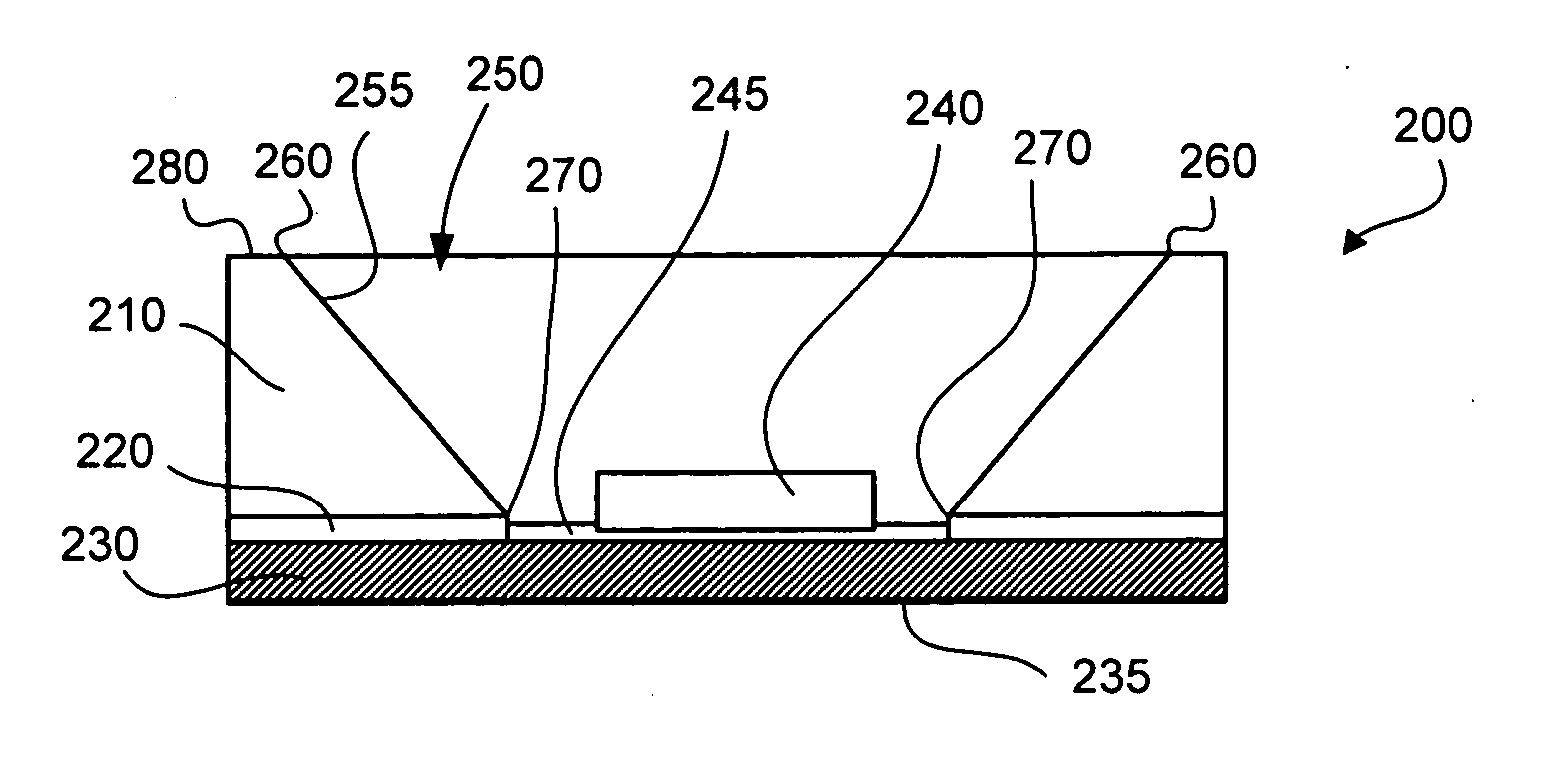
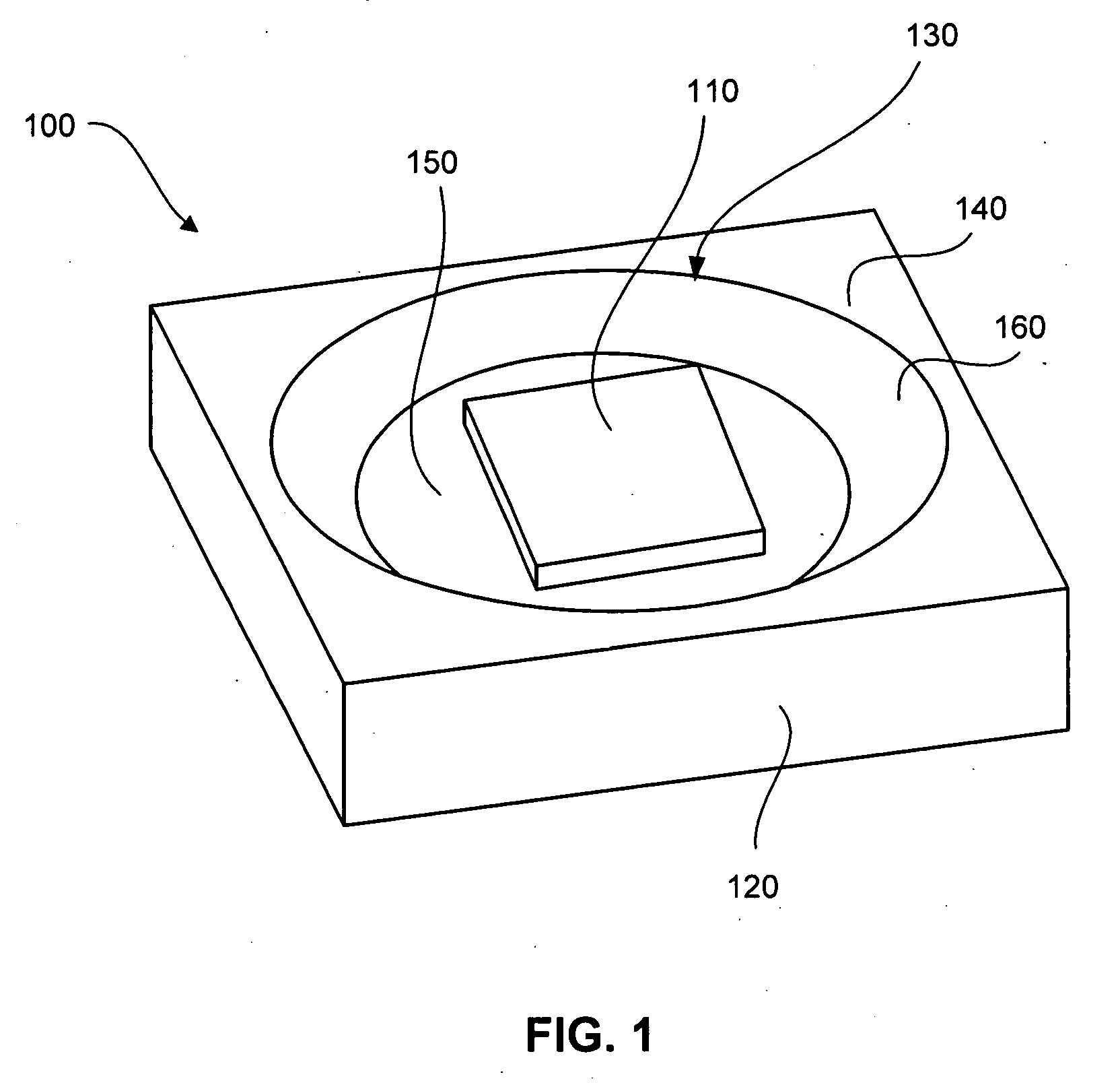
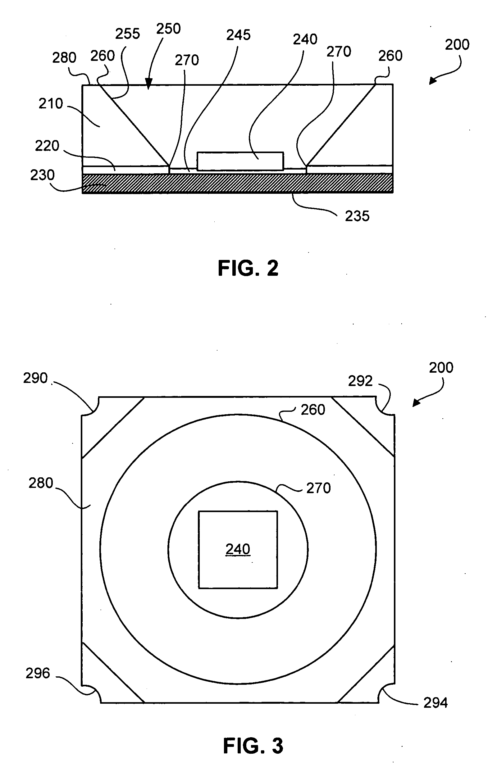
[0028] The present disclosure provides LED packages with structures and materials that provide higher heat dissipation than presently available. A further benefit of the present invention is improved matching of the coefficients of thermal expansion (CTEs) of the LED dies and the materials to which they are bonded for higher reliability. Due to the improved heat conduction, the packages of the present invention allow high-power LEDs to operate at full capacity. Improved heat conduction also allows for both smaller packages and devices within which packages are placed more closely together.

[0029] One measure of how efficiently a package dissipates heat is the temperature rise across the package. Using this measure, in current high-power LED packages the thermal resistance from the junction to the case is generally in the range of 15 to 20° C. / W. By comparison, an exemplary embodiment of the present disclosure has a lower thermal resistance of only about 6° C. / W or 3° ...


PUM

PropertyMeasurementUnit
thicknessaaaaaaaaaa
wavelengthsaaaaaaaaaa
poweraaaaaaaaaa

Abstract

LED packages are provided that include a material that is both thermally conductive and has a coefficient of thermal expansion that is matched to that of an LED. The material can be a ceramic such as aluminum nitride. The package has a body that includes a bottom surface and a cavity disposed into the body. The cavity has a floor for bonding to the LED so that the LED sits within the cavity. The thermally conductive material is disposed between the floor of the cavity and the bottom surface of the package. The body can be fabricated from a number of layers where the thermally conductive material is in a layer disposed between the floor and the bottom surface. The other layers of the body can also be fabricated from the thermally conductive material. A light emitting device is made by attaching the LED to the LED package.

Description

CROSS-REFERENCE TO RELATED APPLICATIONS [0001] The application claims the benefit of U.S. Provisional Patent Application No. 60 / 623,266 entitled “1-5 Watt and Higher LED Packages,” U.S. Provisional Patent Application No. 60 / 623,171 entitled “3-10 Watt and Higher LED Packages,” and U.S. Provisional Patent Application No. 60 / 623,260 entitled “5-15 Watt and Higher LED Packages,” each filed on Oct. 29, 2004 and each incorporated herein by reference in its entirety. The application is related to U.S. patent application Ser. No. ______ (Attorney docket number PA2960US) entitled “High Power LED Package with Universal Bonding Pads and Interconnect Arrangement,” and U.S. patent application Ser. No. ______ (Attorney docket number PA2961US) entitled “Method of Manufacturing Ceramic LED Packages,” both filed on even date herewith. The application is also related to U.S. patent application Ser. No. 11 / 036,559 filed on Jan. 13, 2005 and entitled “Light Emitting Device with a Thermal Insulating an...

Claims


Application Information

Patent Timeline
Patent Type & Authority Applications(United States)
IPC IPC(8): H01L33/00H01L33/60H01L33/64
CPCH01L33/60H01L33/641H01L2924/0002H01L2924/00
Inventor YAN, XIANTAO
Owner LED ENGIN
Why Eureka
Try Eureka