Rite-once high density optical information recording medium
a high density, optical information technology, applied in the field of record media, can solve the problems of irreversible process of above, and achieve the effects of reducing data jitter, good recording characteristics, and improving data quality
- Summary
- Abstract
- Description
- Claims
- Application Information
AI Technical Summary
Benefits of technology
Problems solved by technology
Method used
Image
Examples
embodiment 1
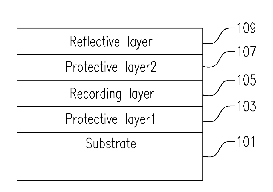
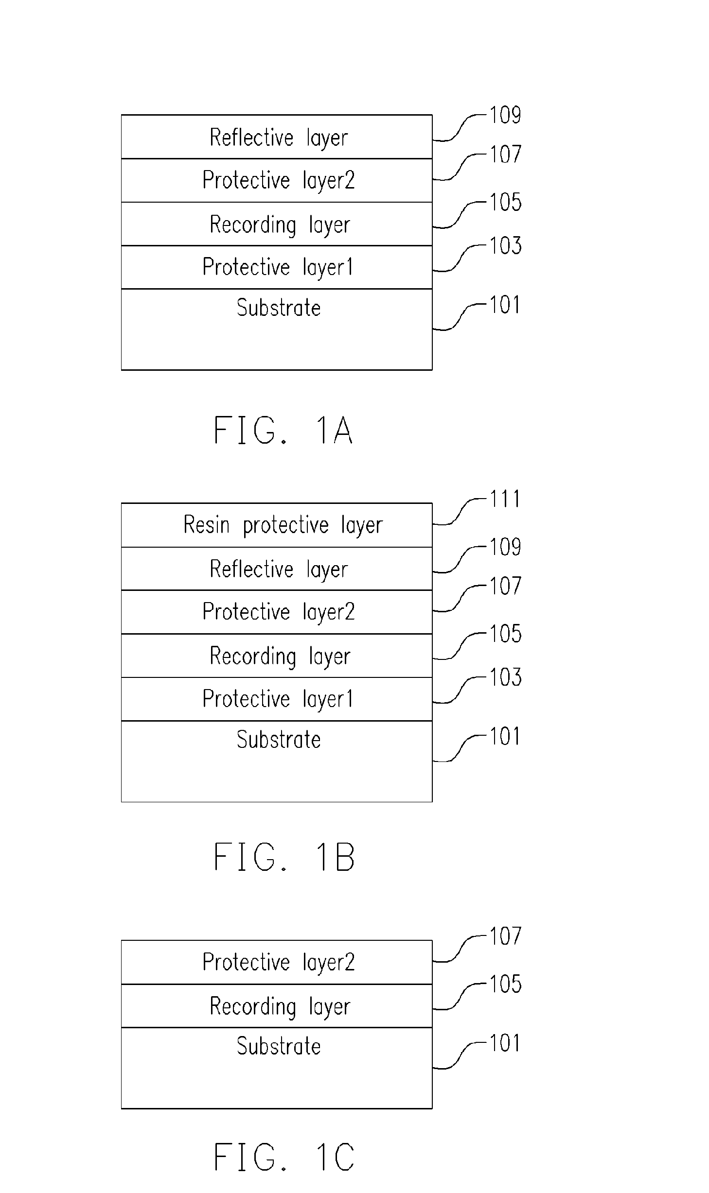
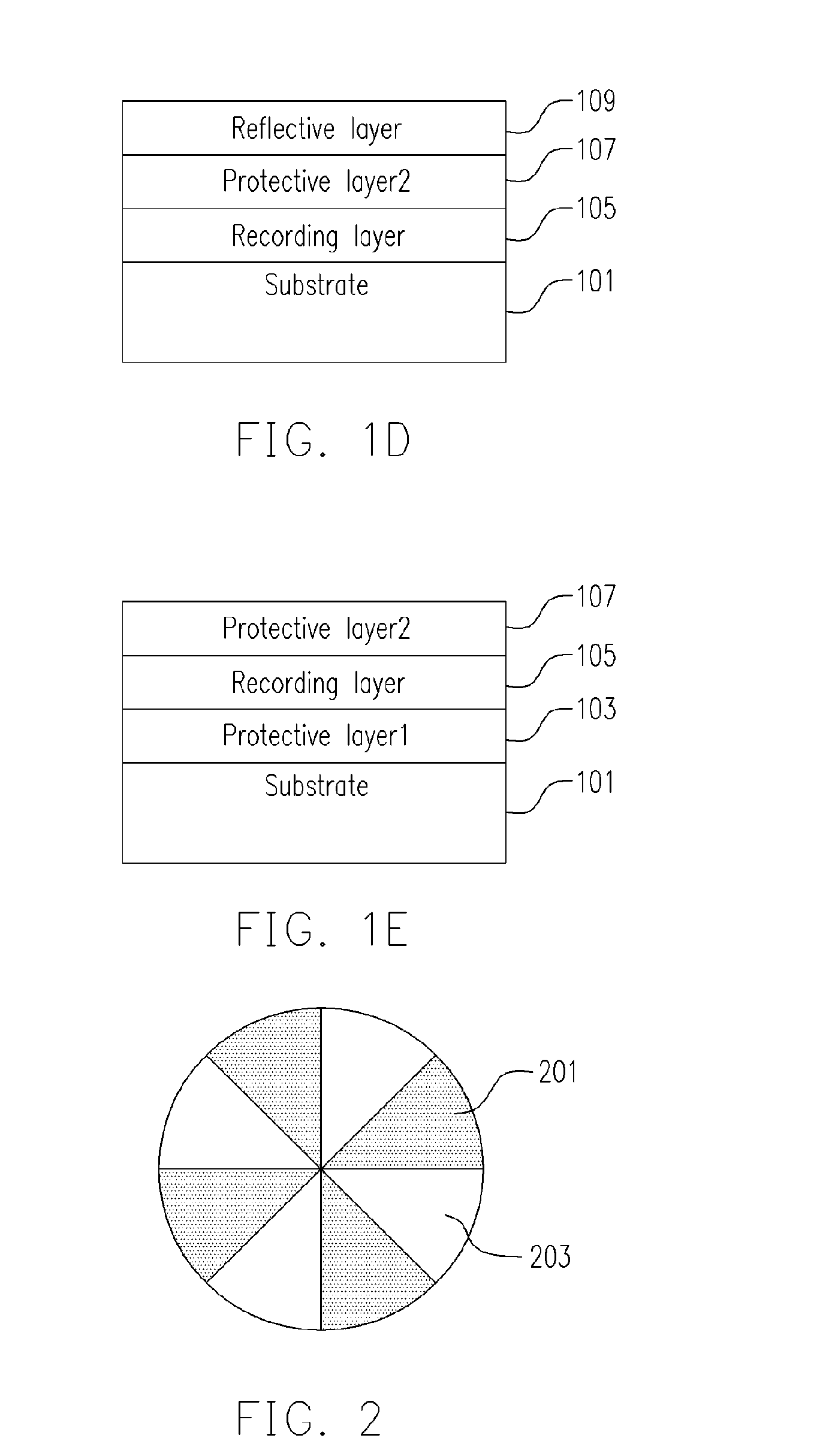
[0038] EMBODIMENT 1, in which the structure of the multiple-layer film of which is as follows:
[0039] 1.1A protective layer (ZnS—SiO2) is formed on the DVD substrate (with track pitch of 0.74 μm) by sputtering;
[0040] 1.2An inorganic material recording layer (SixAly alloy) is formed on the protective layer;
[0041] 1.3Then, a protective layer (ZnS—SiO2) is formed on the inorganic material recording layer, and a reflective layer (AlTi) is formed on the protective layer;
[0042] 2.1EMBODIMENT 2, in which the multiple-layer structure of which is as follows:
[0043] 2.1 A protective layer (ZnS—SiO2) is formed on the optical disc substrate (with track pitch of 0.4 μm) by sputtering;
[0044] 2.2An inorganic material recording layer (SixAlyOz alloy) is formed on the protective layer;
[0045] 2.3 Then, another protective layer (ZnS—SiO2 with thickness of 5 nm-100 nm) is formed on the inorganic material recording layer, and a reflective layer (Ag) is formed on the protective layer;
[0046] The reco...
embodiment 3
[0047] EMBODIMENT 3, in which the structure of the multiple layer film of which is as follows:
[0048] 3.1 A protective layer (ZnS—SiO2) is formed on the optical disc substrate (with track pitch of 0.4 μm) by sputtering;
[0049] 3.2 An inorganic material recording layer (SixAlyNz alloy) is formed on the protective layer;
[0050] 3.3 Then, a protective layer (ZnS—SiO2) is formed on the inorganic material recording layer, and a reflective layer (Ag) is formed on the protective layer;
[0051] The recording characteristics can be remarkably improved by adjusting the gas flow of N2 in the sputtering process of the recording layer of the present invention.
[0052] The protective layer, the recording layer, and the reflective layer of the write-once high density optical information recording medium of the present invention can be formed by consecutive sputtering process, hence the manufacturing process is relatively simple.
[0053] In order to verify the recording characteristics of the high dens...
first embodiment
[0060] Measurement for the testing disc of the first embodiment is performed using the static test apparatus (made by the Toptica company, Model: Media test-1). Marks on the testing disc are recorded by the static test device using one semiconductor red laser diode (wavelength 659 nm) under single pulse mode and monitored by another semiconductor laser diode (wavelength 633 nm) under continuous wave mode. That is, the inorganic material recording layer is irradiated by single laser pulses with different red laser power (mW) and duration time (ns), and the optical properties are measured by continuous laser wave to sow the difference in reflectivity between the recorded mark and non-recorded area throughout the process in which the reflectivity difference is converted to voltage signal to measure the time for the phase conversion. And the recording process is also viewed corresponding to each condition using the charge coupling device (CCD) camera photo image. In which, the recording...
PUM
 Abstract
Description
Claims
Application Information


