Method for treating base oxide to improve high-K material deposition

Inactive Publication Date: 2006-05-04
TAIWAN SEMICON MFG CO LTD
View PDF13 Cites 38 Cited by
  • Summary
  • Abstract
  • Description
  • Claims
  • Application Information

AI Technical Summary

Benefits of technology

[0009] To achieve the foregoing and other objects, and in accordance with the purposes of the present invention, as embodied and broadly described herein, the present invention provides a method for forming a high-K material layer in a semiconductor device fabrication process.
[0010] In a first embodiment, the method includes

Problems solved by technology

Because of high direct tunneling currents, SiO2 films thinner than about 20 Angstroms cannot be reliably used as a gate dielectric in CMOS devices.
There have been, however, difficulties in forming high-k gate dielectrics to achieve acceptable processing integration between the high-K gate dielectric and an underlying base oxide layer or Si substrate.
Since a base oxide can readily form over the silicon from atmospheric exposure and produces a rough deposition surface unsuitable for epitaxy or ALCVD, a silicon wafer cleaning process is typically undertaken to first form a chemically produced oxide surface on the silicon for forming overlying ALCVD layers.
For example, the uniformity of the high-K/semiconductor wafer interface is critical, since the excessive formation of surface defects in the form of, for example, dislocations, provides trapping sites or charge accumulation areas which interfere with acceptable gate dielectric performance.
However, neither the formation of chemically produced oxides on the silicon wafer surface nor the growth of thermal oxides provides a surface quality that is

Method used


Image

  • Method for treating base oxide to improve high-K material deposition
  • Method for treating base oxide to improve high-K material deposition
  • Method for treating base oxide to improve high-K material deposition

Examples


Embodiment Construction

[0017] Although the method of the present invention is explained with reference to the formation of an exemplary high-K gate dielectric stack, it will be appreciated that the method of the present invention may be used for the formation of high-K gate dielectrics for MOSFET devices as well as capacitor stacks in a micro-integrated circuit manufacturing process.

[0018] Although the method of the present invention is explained with reference to the use of exemplary high-k gate dielectrics it will be appreciated that the method of the present invention may be adapted for the use of any high-k material in the formation of a gate dielectric. By the term high-k dielectric is meant a material that has a dielectric constant of greater than about 10. The term “substrate” is defined to mean any semiconductor substrate material including conventional silicon semiconductor wafers.

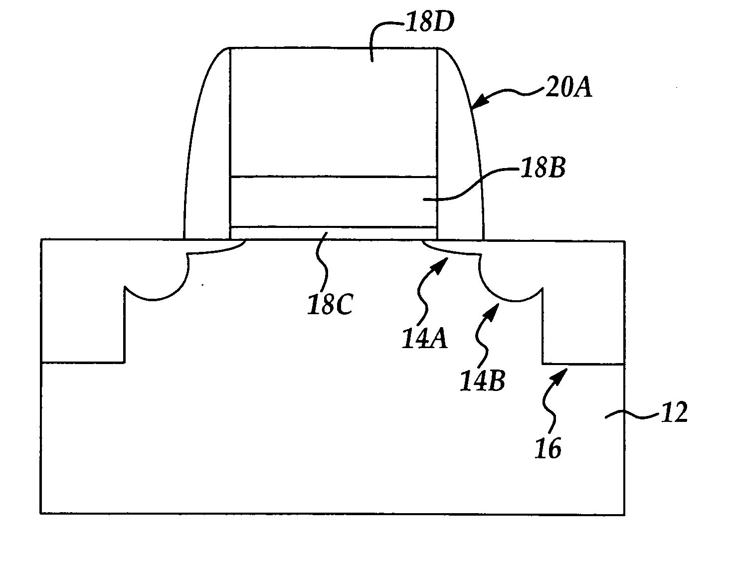
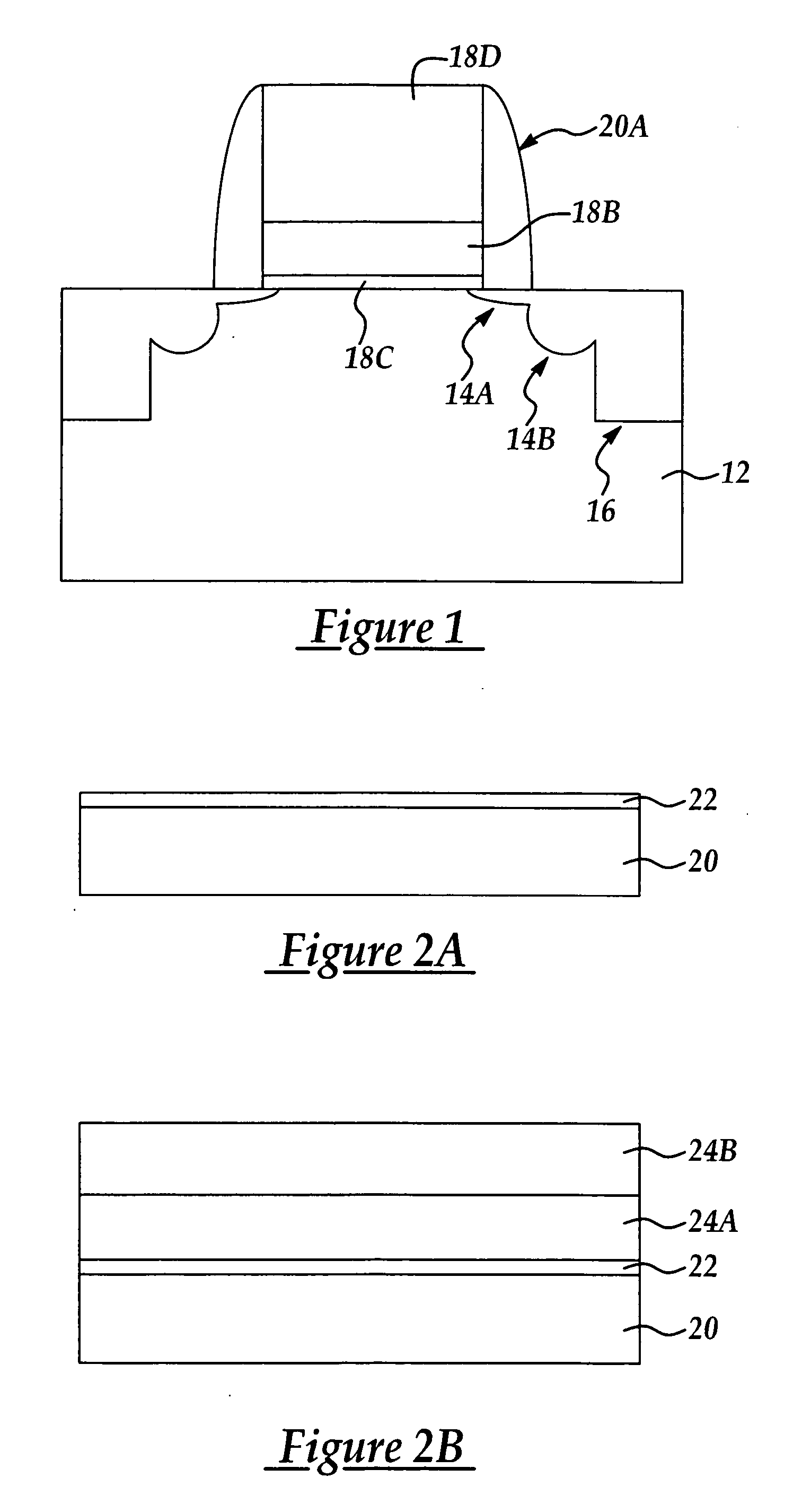
[0019] Referring to FIG. 1A is shown a cross sectional schematic of an exemplary CMOS transistor having a high-k di...


PUM

PropertyMeasurementUnit
Temperatureaaaaaaaaaa
Thicknessaaaaaaaaaa

Abstract

A method for forming a high-K material layer in a semiconductor device fabrication process including providing a silicon semiconductor substrate or thermally growing interfacial oxide layer comprising silicon dioxide over the silicon substrate; treating with an aqueous base solution or nitridation and depositing a high-K material layer.

Description

FIELD OF THE INVENTION [0001] The present invention relates generally to high-K gate stack and capacitor stack fabrication processes in micro-integrated circuit fabrication and more particularly, to a method of treating the base (underlying) oxide or Si substrate to improve the deposition of overlying high-K materials. BACKGROUND OF THE INVENTION [0002] Fabrication of a metal-oxide-semiconductor (MOS) integrated circuit involves numerous processing steps. A gate oxide is typically formed from thermally grown silicon dioxide over silicon or polysilicon which is doped with either n-type or p-type dopants. For each MOS field effect transistor (MOSFET) being formed, a gate electrode is formed over the gate dielectric, and dopant impurities are then introduced into the semiconductor substrate to form source and drain regions. Many modern day semiconductor microelectronic fabrication processes form features having less than 0.25 micron critical dimensions, for example more recent devices ...

Claims


Application Information

Patent Timeline
IPC IPC(8): H01L21/336H01L21/3205C23C16/02H01L21/02H01L21/28H01L21/314H01L21/316H01L21/76H01L29/51H01L29/78
CPCC23C16/0227H01L21/0206H01L21/28185H01L21/28194H01L21/3141H01L21/3144H01L21/31645H01L29/513H01L29/517H01L29/7833H01L21/02307H01L21/02181H01L21/022H01L21/02271H01L21/0228H01L21/02312H01L21/02315
Inventor YANG, MING-HOYAO, LIANG-GEICHEN, SHIH-CHANG
Owner TAIWAN SEMICON MFG CO LTD
Why Eureka
Try Eureka