Chemical mechanical polishing apparatus and chemical mechanical polishing method using the same

Inactive Publication Date: 2006-05-04
DONGBU ELECTRONICS CO LTD
View PDF6 Cites 7 Cited by
  • Summary
  • Abstract
  • Description
  • Claims
  • Application Information

AI Technical Summary

Benefits of technology

[0016] The present invention has been made in an effort to provide a CMP apparatus and method having advantages of improving polishing uniformity by controlling heat generated during a CMP process such that a polishing pad may have a uniform temperature distribution.
[0019] When the polishing pad is a single pad, the plurality of metal lines may be formed at or on the bottom side of the polishing pad, such that corrosion by cleaning water or a chemical such as one in a slurry may be prevented.
[0021] According to such a CMP apparatus, the heat generated at a central region of a wafer may be rapidly conducted to a peripheral region thereof, and thus a temperature distribution in or of the polishing pad may be substantially uniform.

Problems solved by technology

However, such efforts to improve polishing uniformity have been satisfactory only to a limited degree, for the following reasons.
Such a phenomenon results in a bigger difference in the removal rate between the central region and the peripheral region as the wafer becomes larger in diameter.
Furthermore, planarization of a metal layer for forming a metal line produces greater frictional heat in comparison with planarization of an oxide layer, and in this case the polishing uniformity becomes worse.
However, such a conventional method may only provide a mere effect of lowering the temperature of the platen, rather than enabling the temperature distribution of a wafer surface to be more uniform.
Therefore, polishing uniformity that may be achieved by such a conventional method is not sufficient for an improvement of the polishing uniformity.

Method used


Image

  • Chemical mechanical polishing apparatus and chemical mechanical polishing method using the same
  • Chemical mechanical polishing apparatus and chemical mechanical polishing method using the same
  • Chemical mechanical polishing apparatus and chemical mechanical polishing method using the same

Examples


Embodiment Construction

[0034] Exemplary embodiments of the present invention will hereinafter be described in detail with reference to the accompanying drawings.

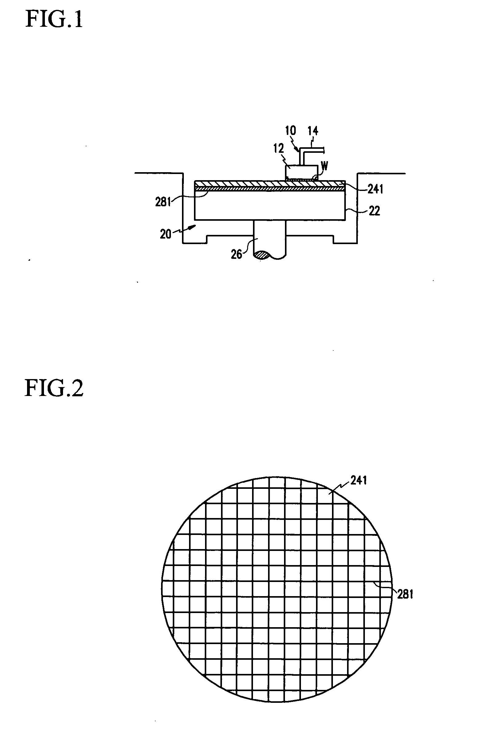
[0035]FIG. 1 is a schematic diagram of a CMP apparatus according to an exemplary embodiment of the present invention, and FIG. 2 shows a bottom view of a polishing pad in FIG. 1.

[0036] As shown in FIG. 1, a CMP apparatus according to the present exemplary embodiment includes a polishing head assembly 10 and a polishing station 20.

[0037] The polishing head assembly 10 includes a polishing head 12 holding a wafer W and an arm 14 connected with the polishing head 12.

[0038] Here, the polishing head 12 may fixedly hold the wafer W by vacuum, generated by a vacuum generator (not shown). In this case, the polishing head 12 may include a membrane, a retainer ring, and a carrier. Here, the membrane makes surface contact with a rear side of the wafer W and expands by compressed air supplied through a fluid hole of a carrier, and it thereby applies a for...


PUM

PropertyMeasurementUnit
Widthaaaaaaaaaa
Thermal conductivityaaaaaaaaaa
Distributionaaaaaaaaaa

Abstract

Polishing uniformity in a CMP process may be improved due to an improvement in the temperature uniformity of a polishing surface, when a wafer is polished by a CMP apparatus including a polishing head for holding the wafer, a platen, a polishing pad at a top of the platen so as to polish the wafer, and a heat conduction medium on or in the polishing pad and configured to diffuse heat of the polishing pad such that the temperature distribution of the polishing pad may become substantially uniform.

Description

CROSS-REFERENCE TO RELATED APPLICATION [0001] This application claims priority to and the benefit of Korean Patent Application No. 10-2004-0087868, filed in the Korean Intellectual Property Office on Nov. 1, 2004, the entire contents of which are incorporated herein by reference. BACKGROUND OF THE INVENTION [0002] (a) Field of the Invention [0003] The present invention relates to a chemical mechanical polishing (CMP) apparatus and a CMP method using the same. [0004] (b) Description of the Related Art [0005] Recently, with the high integration of semiconductor devices, the structure thereof has been multi-layered. Accordingly, a polishing process for planarizing layers of a semiconductor wafer is typically included in a fabrication process of the semiconductor devices. As such a polishing process, a chemical mechanical polishing (CMP) process is widely adopted. [0006] The CMP process is a process for polishing a surface of a wafer coated with an oxide or metal such as tungsten, coppe...

Claims


Application Information

Patent Timeline
IPC IPC(8): B24B51/00B24B1/00
CPCB24B37/24B24B49/14H01L21/304
Inventor KIM, WAN-SHICK
Owner DONGBU ELECTRONICS CO LTD
Why Eureka
Try Eureka