Semiconductor device

a technology of semiconductors and semiconductors, applied in the field of semiconductor devices, can solve the problems of difficult data reading, high tamper resistance of stored data, and data leakage, and achieve the effects of flexible circuit structure, reduced risk of data leakage, and high speed

a technology of semiconductors and semiconductors, applied in the field of semiconductor devices, can solve the problems of difficult data reading, high tamper resistance of stored data, and data leakage, and achieve the effects of flexible circuit structure, reduced risk of data leakage, and high speed

US20060095975A1Inactive Publication Date: 2006-05-04PANASONIC CORP

Image

  • Semiconductor device
  • Semiconductor device
  • Semiconductor device

Examples


first embodiment

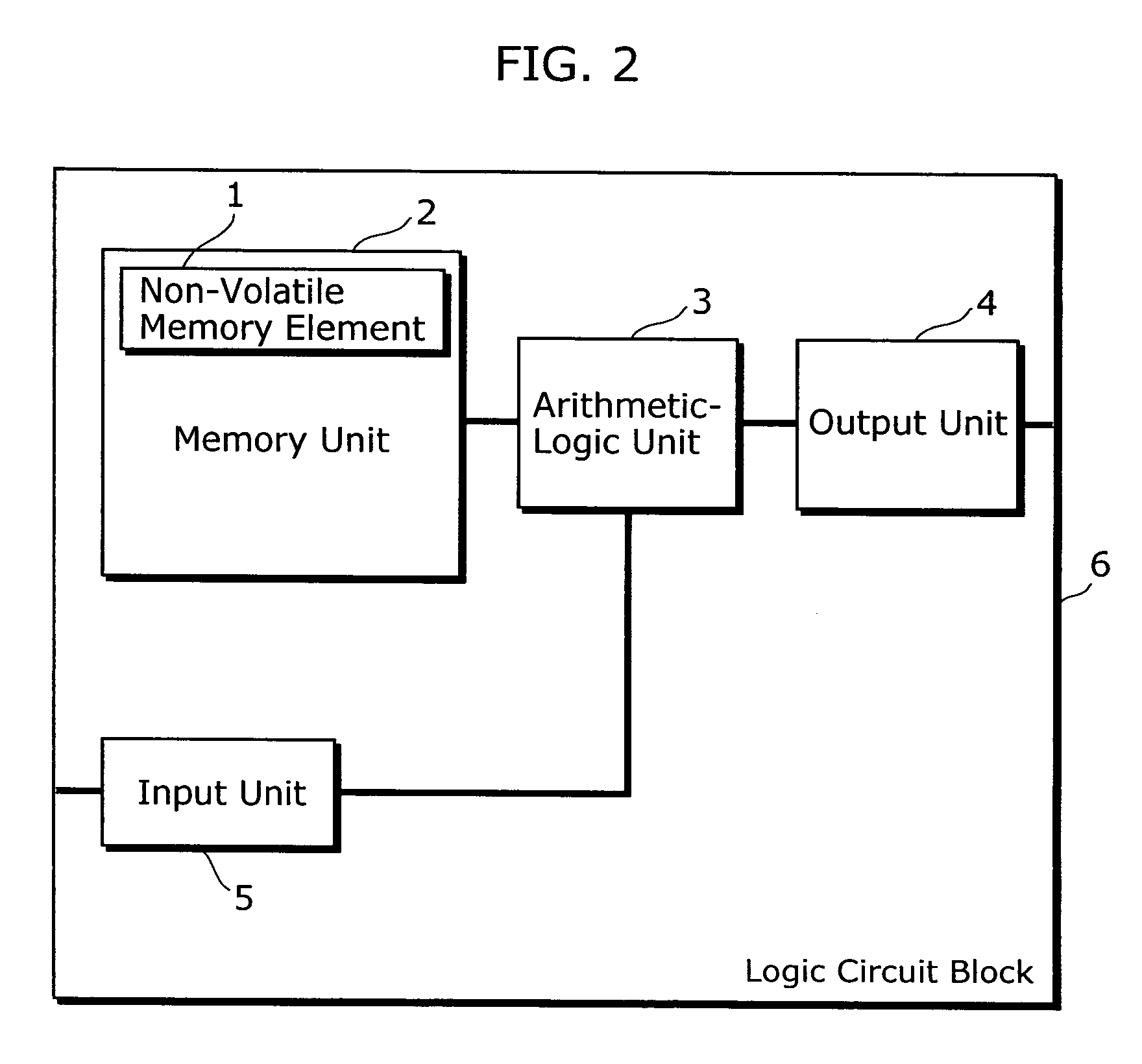
[0075]FIG. 2 is a block diagram showing a structure of a logic circuit block in a semiconductor device according to the first embodiment of the present invention. A logical circuit block 6 in the semiconductor device according to the first embodiment of the present invention is comprised of: a non-volatile memory unit 2 that has a non-volatile memory element 1 for storing data; an arithmetic-logic unit 3 that performs arithmetic-logic operations using data stored in the memory unit 2 and data inputted from the outside via an input unit 5; and an output unit 4 that outputs an arithmetic-logic result generated by the arithmetic-logic unit 3, all of which are integrated as a single functional block. Here, an output line of the memory unit 2 is connected only to the arithmetic-logic unit 3.

[0076] With the above structure, the data stored in the memory unit 2 is outputted only to the arithmetic-logic unit 3, there is no path for outputting the data stored in the memory unit 2 to the out...

second embodiment

[0099]FIG. 9 is a block diagram showing a structure of a semiconductor device according to the second embodiment of the present invention. A semiconductor device 100 in FIG. 9 is comprised of an processing element array (hereafter, the processing element array will be referred to as PE array, and a processing element will be referred to as PE.) 101, an input buffer 102, an output buffer 103, an address buffer 104, a row decoder 105, a column decoder 106, a read / write amplifier (hereafter, referred to as RW amplifier) 108, a shift register 109, and a control circuit 110. The semiconductor device 100 is implemented using the FPGA by which functions in the circuit can be programmed to be changed.

[0100] As shown in FIG. 10, the PE array 101 is comprised of a plurality of the PEs 11 which are regularly arranged on a matrix.

[0101] The following describes how to program the PE array 101. Configuration data is outputted from an external write device 200 to the RW amplifier 108 via the shi...


PUM


Abstract

A semiconductor device of the present invention includes: at least one of non-volatile memory unit operable to store data; at least one of an arithmetic-logic unit operable to perform an arithmetic-logic operation using data which is stored in the memory unit and data that is inputted from outside; and an output unit operable to output a result of arithmetic-logic operation performed by the arithmetic-logic unit; wherein the memory unit, the arithmetic-logic unit, and the output unit are included in a functional block, and an output line of each of the memory unit is connected only to one of at least one of the arithmetic-logic unit.

Description

BACKGROUND OF THE INVENTION [0001] (1) Field of the Invention [0002] The present invention relates to a semiconductor device which is comprised of a logic circuit having non-volatile memory elements. [0003] (2) Description of the Related Art [0004] In recent years, various system large-scale integrations (LSI) have been developed to arrange non-volatile memory cores together with a large-scale logic circuit, a microcomputer, and the like, on a single chip. To realize such a system LSI at low cost and with multiple functions, it is effective to apply a method for embedding various functional blocks on a single chip to decrease the total number of chips, thereby reducing an assembling cost. [0005] Moreover, there have recently been increased necessities of storing programs, cords, and the like into the LSI, and of storing highly confidential data such as passwords. For example, as shown in FIG. 1A, the LSI includes an input / output unit 4 and a memory unit 2 having a non-volatile memor...

Claims


Application Information

Patent Timeline
04 May 2006
Publication
US20060095975A1
IPC
H04L9/32
CPC
G06F21/75; G06F21/79; H04L9/085
Inventors
YAMADA, TAKAYOSHI; KOYAMA, SHINZO