Semiconductor chip capable of implementing wire bonding over active circuits

a technology of active circuits and semiconductors, applied in the direction of semiconductor devices, semiconductor/solid-state device details, electrical apparatus, etc., can solve the problems of weak supporting structure, inability to reduce the chip size, and inability to implement wire bonding over active circuits, etc., to achieve the effect of simplifying the manufacturing process

Active Publication Date: 2006-05-18
UNITED MICROELECTRONICS CORP
View PDF16 Cites 26 Cited by
  • Summary
  • Abstract
  • Description
  • Claims
  • Application Information

AI Technical Summary

Benefits of technology

[0010] Since the metal-metal capacitor of the present invention is formed by a pair of same plane metal electrodes, it is able to be formed by one standard copper damascene process for simplifying the manufacturing process. Furthermore, the present invention utilizes a plurality of pairs of same plane metal electrodes vertically stacked to form metal-metal capacitors, so a large number of electric charges are capable of being stored in the metal-metal capacitors of the present invention and the capacitor structure of the present invention is a good reinforcement supporting structure for protecting active circuits situated beneath it.

Problems solved by technology

Therefore, bonding pads which spread around on a chip are obstacles for reducing the chip size.
However, U.S. Pat. No. 6,476,459 has disadvantages of the supporting structure being weaker and the manufacturing process being too complex.

Method used


Image

  • Semiconductor chip capable of implementing wire bonding over active circuits
  • Semiconductor chip capable of implementing wire bonding over active circuits
  • Semiconductor chip capable of implementing wire bonding over active circuits

Examples


Embodiment Construction

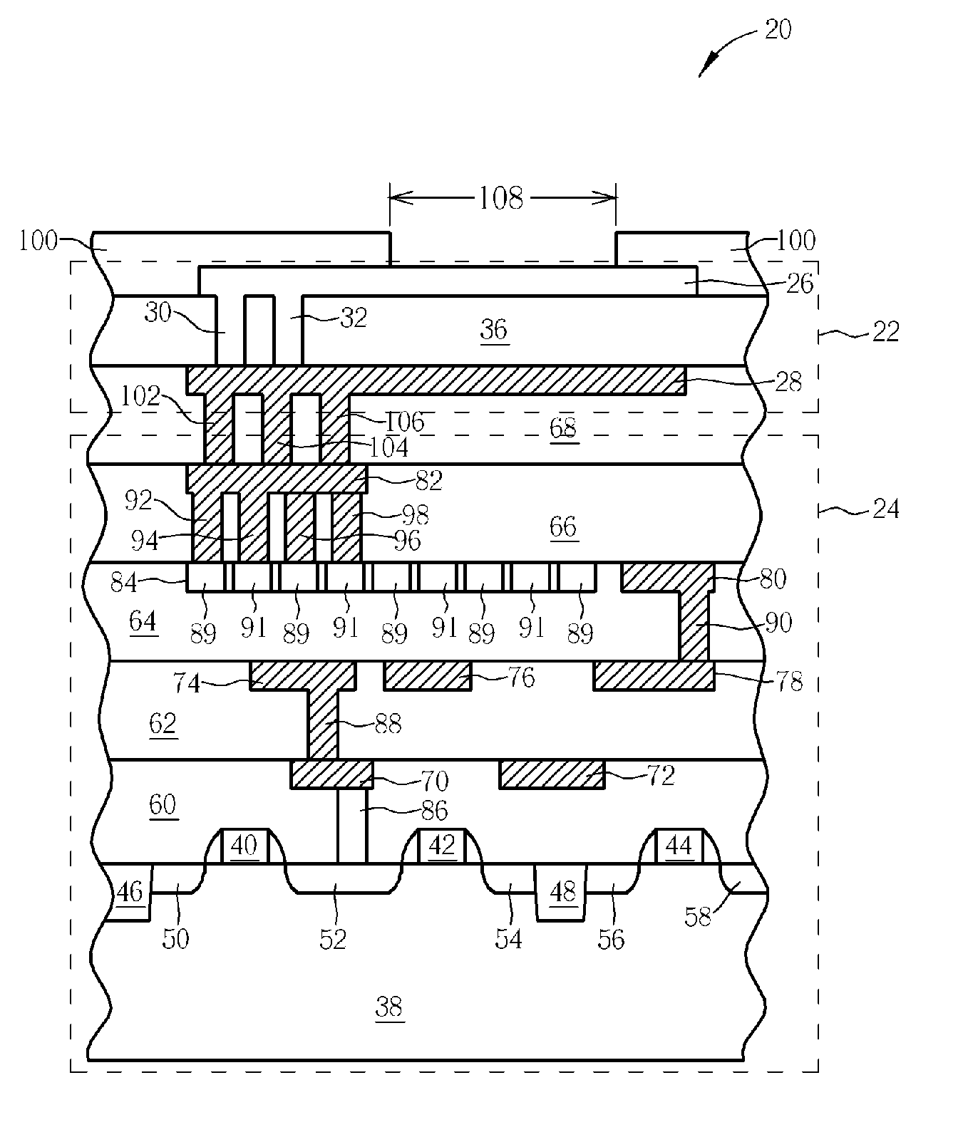
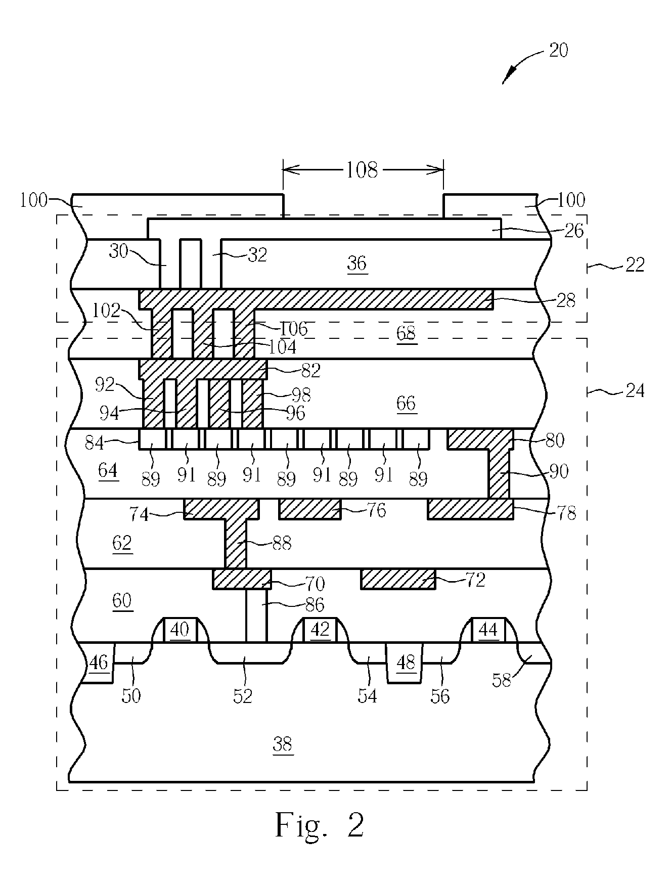
[0016] Please refer to FIG. 2. FIG. 2 is a schematic cross-sectional diagram of a BOAC integrated circuit structure 20 according to a first embodiment of the present invention. As shown in FIG. 2, a BOAC integrated circuit structure 20 of the present invention includes a bonding pad structure 22 and an active circuit region 24. The bonding pad structure 22, which is a reinforcement structure, includes a bondable metal pad 26, a top interconnection metal layer 28, first via plugs 30 and 32 located beneath the bondable metal pad 26 for electrically linking the bondable metal pad 26 with the top interconnection metal layer 28, and a stress-buffering dielectric 36 located between the bondable metal pad 26 and the top interconnection metal layer 28.

[0017] The active circuit region 24 may include input / output (I / O) devices / circuits or electrostatic discharge (ESD) devices / circuits on a semiconductor substrate 38, and include metal-oxide-semiconductor field-effect transistors (MOSFET) 40,...


PUM


Abstract

A semiconductor chip capable of implementing wire bonding over active circuits (BOAC) is provided. The semiconductor chip includes a bonding pad structure, a metal-metal capacitor formed by at least a pair of metal electrodes on the same plane underneath the bonding pad structure, at least an interconnection metal layer, at least a via plug between the interconnection metal layer and the bonding pad structure, and an active circuit situated underneath the bonding pad structure on a semiconductor bottom.

Description

BACKGROUND OF INVENTION [0001] 1. Field of the Invention [0002] The present invention relates to the field of semiconductor integrated circuits, and more particularly, to a semiconductor chip capable of implementing wire bonding over active circuits (also referred to as “BOAC”) and including capacitors situated beneath a bonding pad structure. [0003] 2. Description of the Prior Art [0004] Accompanying progress of semiconductor technology, critical dimensions of integrated circuits are continually shrunk. Therefore, bonding pads which spread around on a chip are obstacles for reducing the chip size. A person skilled in the art understands that active circuits in general are not permitted to be disposed underneath a bonding pad since chip manufacturers and designers agree on the need to avoid damaging integrated circuits disposed underneath a bonding pad with mechanical stress during bonding. Furthermore, the requirements for functional chips and system on a chip (SOC) have increased ...

Claims


Application Information

Patent Timeline
Patent Type & Authority Applications(United States)
IPC IPC(8): H01L23/48
CPCH01L23/5223H01L2224/02166H01L24/06H01L2224/05093H01L2224/05624H01L2924/01013H01L2924/01014H01L2924/01029H01L2924/05042H01L2924/13091H01L2924/14H01L2924/19041H01L24/05H01L2924/01033H01L2924/00014H01L2224/05553
Inventor WU, BING-CHANG
Owner UNITED MICROELECTRONICS CORP
Why Eureka
Try Eureka