Bootstrap circuit and driving method thereof

Active Publication Date: 2006-05-18
GOLD CHARM LTD
View PDF3 Cites 25 Cited by
  • Summary
  • Abstract
  • Description
  • Claims
  • Application Information

AI Technical Summary

Benefits of technology

[0034] According the present invention, a voltage that changes due to the bootstrap effect can be determined independently of the threshold voltage of a transistor, and therefore the influence of manufacturing variations in transistors can be reduced. Accordingly, a circuit with a small range of manufacturing variations and high reliability can be provided.
[0035] Further, according to the present invention, the amount of change in the voltage due to the bootstrap effect can be made small. Accordingly, the voltage to be app

Problems solved by technology

However, the manufacture of a CMOS semiconductor device requires multiple processes of impurity implantation to form PMOS and NMOS, in addition to other processes such as film formation, mask exposure, and etching.
Accordingly, there arises a problem of an increase in cost.
However, because of a single conductivity type of semiconductor, there arise problems that the power consumption increases and the output margin decreases as compared with the CMOS transistor.
That is, in the case where Vthmin is small and hence variations in threshold voltage are wide, there is a possibility that the conduction characteristic may become insufficient.
The same problem also arises in the case of NMOS transistors.
Therefore, if the transis

Method used


Image

  • Bootstrap circuit and driving method thereof
  • Bootstrap circuit and driving method thereof
  • Bootstrap circuit and driving method thereof

Examples


Example

1. First Embodiment

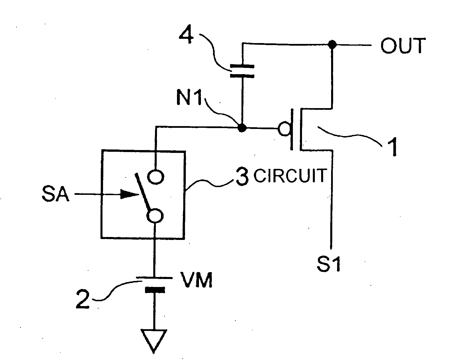
[0067] Referring to FIG. 2, a bootstrap circuit according to a first embodiment of the present invention includes a P-channel MOS (PMOS) transistor 1 that outputs pulses, a coupling capacitor 4 connected between the source electrode (output OUT) and gate electrode (node N1) of the transistor 1, a power source 2 that outputs a DC voltage VM, and a circuit 3 for controllably applying the potential VM to the gate electrode of the transistor 1.

[0068] A pulse signal S1 to be inputted to the drain electrode of the transistor 1 is a pulse signal of a high potential VH and a low potential VL. The circuit 3 has a function of connecting the power source 2 to the node N1 of the transistor 1 to apply the potential VM when a pulse signal SA is at a high level, and a function of disconnecting the power source 2 from the node N1 when SA is at a low level. Here, as a characteristic of the PMOS transistor 1, it is assumed that the transistor 1 is brought into a conductive state ...

Example

2. Second Embodiment

[0072] Referring to FIG. 4, a bootstrap circuit according to a second embodiment of the present invention includes a PMOS transistor 1 that outputs pulses, a coupling capacitor 4 provided between the source electrode (output OUT) and gate electrode (node N1) of the transistor 1, a power source 2 that outputs a voltage of VM, a circuit 3 for controllably applying the potential VM to the node N1, a power source 5 that outputs a voltage of VN, and a circuit 6 for controllably applying the potential VN to the node N1.

[0073] A pulse signal S1 to be inputted to the drain electrode of the transistor 1 is a pulse signal of a high potential VH and a low potential VL. The circuit 3 has a function of connecting the power source 2 to the node N1 to apply the potential VM to the node N1 when a pulse signal SA is at a high level, and a function of disconnecting the power source 2 from the node N1 when SA is at a low level. The circuit 6 has a function of connecting the power...

Example

3. Third Embodiment

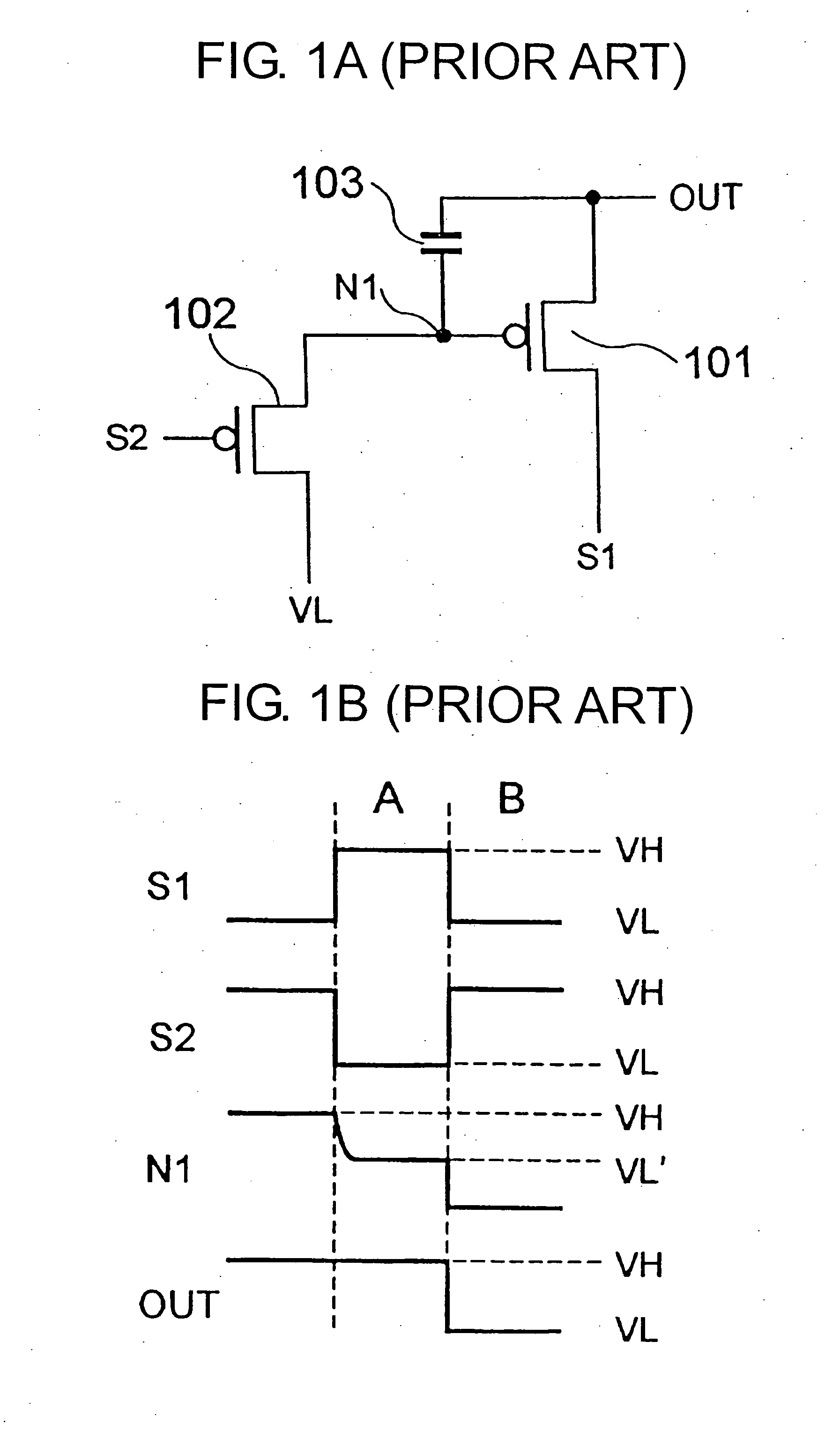
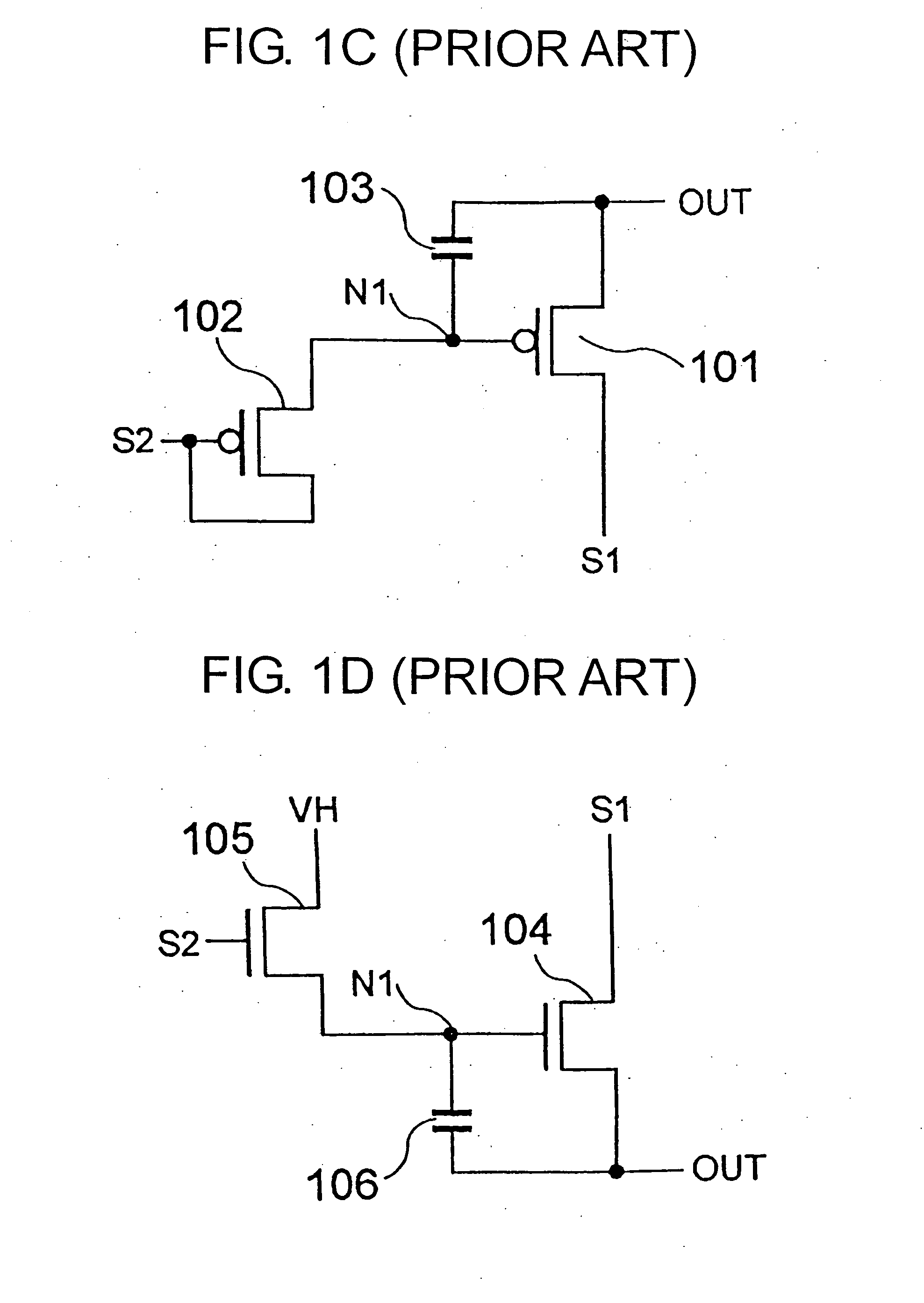
[0081]FIG. 6 shows a bootstrap circuit according to a third embodiment of the present invention, in which the circuit 3 in the bootstrap circuit described in the first embodiment is composed of a specific transistor. In the present embodiment, the circuit 3 is composed of a PMOS transistor 7 having the source and drain electrodes that are connected to the node N1 and the power source 2, respectively. Here, it is assumed that the PMOS transistor 7 is in a conductive state when a pulse signal S2 is at a low level VLL and in a non-conductive state when S2 is at a high level VHH.

[0082] Referring to FIG. 7, the above bootstrap circuit is driven. First, during a period A, since S2 is at the low level VLL, the PMOS transistor 7 is brought into a conductive state, and the initial potential of the node N1 is charged to VM. In the period A, during which the pulse signal S1 is at the high potential VH, since the gate potential is VM, the condition for the conduction of the...


PUM


Abstract

A bootstrap circuit includes an output transistor, a bootstrap capacitor provided between the gate and source of the output transistor, a power source, and a circuit that performs ON/OFF control of a supply from the power source to the gate electrode of the transistor. An initial voltage before a bootstrap effect can be set to the potential of the power source, which is independent of the threshold voltage of the transistor. Therefore, the source output of the transistor rising or dropping due to the bootstrap effect is not affected by variations that depend on the threshold voltage of the transistor.

Description

BACKGROUND OF THE INVENTION [0001] 1. Field of the Invention [0002] The present invention relates to a bootstrap circuit and a method for driving the bootstrap circuit, and also to a shift register circuit, a logical operation circuit, and a semiconductor device each using the bootstrap circuit. More particularly, the present invention relates to a semiconductor device including a circuit that outputs digital pulses, such as a shift register for driving a display device, a camera and the like and an address decoder for driving a memory device. [0003] 2. Description of the Related Art [0004] For a circuit constituting a semiconductor device, in many cases, a CMOS (Complementary Metal-Oxide Semiconductor) circuit using an N-channel MOS (NMOS) transistor and a P-channel MOS (PMOS) transistor is generally employed because of its low power consumption. In a CMOS circuit, when digital pulses are outputted, high and low levels of potential can be outputted by using high potential (VH) and ...

Claims


Application Information

Patent Timeline
IPC IPC(8): H03K19/094H03K19/0175
CPCG09G3/3677H03K17/063H03K19/01735
Inventor NONAKA, YOSHIHIRO
Owner GOLD CHARM LTD
Why Eureka
Try Eureka