Resist material for liquid immersion lithography process and method for forming resist pattern using the resist material

a liquid immersion lithography and resist material technology, applied in the field of resist materials, can solve the problems of shortening the wavelength of the light source, requiring an expensive new apparatus, and reducing the focal depth range, so as to improve the resolution of the resist pattern

Inactive Publication Date: 2006-05-25
TOKYO OHKA KOGYO CO LTD
View PDF3 Cites 7 Cited by
  • Summary
  • Abstract
  • Description
  • Claims
  • Application Information

AI Technical Summary

Benefits of technology

[0012] In the above invention, it is preferable to enhance the resolution of the resist pattern by exposing a resist film to light with an intervening liquid with a predetermined thickness whose refractive index is higher than that of air and lower than that of the resist film on at least the resist film in a path of the lithography exposure light reaching the resist film.
[0057] By forming the resist pattern in this way, it is possible to produce the resist pattern having a fine line width, particularly a line and space pattern with small pitch which shows the good resolution.

Problems solved by technology

However, the shortening of the wavelength of the light source requires an expensive new apparatus.
In the increase of the numerical aperture, there is a problem that even when the resolution is increased, a focal depth range is decreased because the resolution and the focal depth range are in trade-off relationship.

Method used


Image

  • Resist material for liquid immersion lithography process and method for forming resist pattern using the resist material
  • Resist material for liquid immersion lithography process and method for forming resist pattern using the resist material
  • Resist material for liquid immersion lithography process and method for forming resist pattern using the resist material

Examples


example 1

[0060] A negative resist material whose solid weight was 8.1% by weight was prepared by dissolving a resin component having a repeat unit represented by the following chemical formula (5):

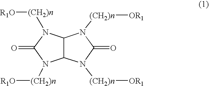
wherein m:n is 84:16 (mol %), 10% by weight of a water-poorly soluble crosslinker composed of tetrabutoxymethylated glycoluril, 1% by weight of an acid generator composed of triphenylsulfonium nonafluorobutanesulfonate and 0.6% by weight of an amine component composed of 4-phenylpyridine based on the weight of the resin component in propylene glycol monomethyl ether.

[0061] On the other hand, an organic anti-reflection film with a thickness of 82 nm was formed by applying the organic anti-reflection film “AR-19” (trade name, supplied from Shipley) on a silicon wafer which was a substrate using a spinner and baking at 215° C. for 60 seconds on a hotplate to dry. A resist film with a thickness of 250 nm was formed on this anti-reflection film by applying the aforementioned negative resist material...

example 2

[0065] A resist pattern was obtained by employing the aforementioned evaluation test that “the resist film is showered with the immersion liquid (purified water) after the exposure, and subsequently developed to inspect the resolution of the resulting resist pattern”, giving the exposure using a substrate with the same constitution as in Example 1 and using the same light source as in Example 1, showering with the purified water for 120 seconds, and subsequently performing the PEB treatment and development in the same way as in Example 1.

[0066] The resist pattern having 160 nm line-and-space at 1:1 obtained in this way was observed by the scanning electron microscope (SEM), and consequently, the pattern was preferable because no pattern defect such as swelling was observed in its profile. The sensitivity at that time was 30.7 mJ / cm2. Meanwhile, when a resist pattern was formed using the resist material in Example 2 by the conventional formation method without giving the showering t...

example 3

[0067] A negative resist material whose solid weight was 7.0% by weight was prepared by dissolving a resin component having a repeat unit represented by the following chemical formula (6):

wherein 1:m:n is 12:44:44 (mol %), 10% by weight of a water-poorly soluble crosslinker composed of tetrabutoxymethylated glycoluril, 1.5% by weight of an acid generator composed of triphenylsulfonium perfluorobutanesulfonate and 0.2% by weight of an amine component composed of triethanolamine based on the weight of the resin component in propylene glycol monomethyl ether.

[0068] On the other hand, an organic anti-reflection film with a thickness of 82 nm was formed by applying the organic anti-reflection film “AR-19” (trade name, supplied from Shipley) on a silicon wafer which was a substrate using the spinner and baking at 215° C. for 60-seconds on the hotplate to dry. A resist film with a thickness of 150 nm was formed on this anti-reflection film by applying the aforementioned negative resist...


PUM

PropertyMeasurementUnit
widthaaaaaaaaaa
thicknessaaaaaaaaaa
thicknessaaaaaaaaaa

Abstract

A negative resist material for a liquid immersion lithography process containing a resin component and a crosslinker component for this resin component, wherein the crosslinker component is poorly soluble in a liquid immersion medium, and a method for forming a resist pattern by the use thereof are provided. These simultaneously prevent alteration of a resist film and alteration of the liquid used during the liquid immersion lithography and enable to form the resist pattern with high resolution using the liquid immersion lithography. In the liquid immersion lithography process, the resolution of the resist pattern is enhanced by exposing the resist film to light with the intervening liquid with a predetermined thickness whose refractive index is higher than that of air and lower than that of the resist film on at least the resist film in a path of lithography exposure light reaching the resist film.

Description

TECHNICAL FIELD [0001] The present invention relates to a resist material which is preferable for obtaining a resist film used for a liquid immersion lithography process, in particular, the liquid immersion lithography process in which a resolution of the resist pattern is enhanced by exposing the resist film to light with an intervening liquid with a predetermined thickness whose refractive index is higher than that of air and lower than that of the resist film on at least the resist film in a path of the lithography exposure light reaching the resist film, and a method for forming a resist pattern using the resist material. BACKGROUND ART [0002] Lithographic methods are frequently used for manufacturing fine structures in various electronic devices such as semiconductor devices and liquid crystal devices, and microfabrication is also required for resist patterns in lithographic processes along with the microfabrication of device structures. [0003] Currently, it is possible to form...

Claims


Application Information

Patent Timeline
Patent Type & Authority Applications(United States)
IPC IPC(8): G03C1/76G03F7/038G03F7/20G03F7/004H01L21/027
CPCG03F7/2041G03F7/038
Inventor IWASHITA, JYUNHIRAYAMA, TAKUTACHIKAWA, TOSHIKAZU
Owner TOKYO OHKA KOGYO CO LTD
Why Eureka
Try Eureka