Self-aligned trench filling with high coupling ratio

a trench filling and high coupling ratio technology, applied in the field of high density semiconductor devices, can solve the problems of stress and ultimately defects in silicon, the space available for isolating devices tends to decrease, and the parasitic current and charge of inter-devices can become more problematic, so as to achieve greater width and depth.

Active Publication Date: 2006-05-25
SANDISK TECH LLC
View PDF63 Cites 32 Cited by
  • Summary
  • Abstract
  • Description
  • Claims
  • Application Information

AI Technical Summary

Benefits of technology

[0009] Self-aligned trench filling to isolate active regions in high-density integrated circuits is provided. A deep, narrow trench is etched into a substrate between active regions. The deep, narrow trench can form an effective isolation region between active regions without occupying as much lateral substrate area as required by other techniques such as shallow trench isolation. The trench is filled by growing a suitable dielectric such as silicon dioxide. The dielectric grows from the substrate to fill the trench and into the substrate to provide a dielectric of greater width and depth than the trench. Storage elements for a NAND type flash memory system, for example, can be fabricated by etching the substrate to form the trench after or as part of etching to form NAND string active areas. This technique stands in contrast to prior art techniques (e.g., LOCOS) where the trench is formed prior to device active areas such as a NAND string active area. This can ensure alignment of the NAND string active areas between isolation trenches. Because the dielectric growth process is self-limiting, an open area resulting from the etching process can be maintained between the stacks. A subsequently formed inter-gate dielectric layer and control gate layer can fill the open area to provide sidewall coupling between control gates and floating gates. In prior art techniques that employ deposition to fill trenches, the area between NAND string active areas is filled with the dielectric that is deposited for the trench such that the control gate only overlies the floating gate in a vertical direction. There can be no sidewall coupling in such prior art configurations.

Problems solved by technology

As the density of integrated circuits continues to increase, the space available for isolating devices tends to decrease.
With decreased device dimensions, inter-device parasitic currents and charges can become more problematic, making isolation technology a critical component of integrated circuit fabrication.
This encroachment can cause stresses and ultimately defects in the silicon.
Furthermore, the encroachment decreases the available active area for constructing devices which limits the density that can be achieved in the integrated circuit.
Additionally, the LOCOS technique can cause alignment issues since the trench is formed prior to forming layers such as the conductive layer used to fabricate the floating gate of a device.
For example, the subsequently formed floating gate material may not properly align between two predefined trenches.
While this process provides an improvement to conventional LOCOS, the nitride in the trench rises during oxidation, causing encroachment into the active areas.
This technique also yields excessive stress in the corners of the trench since oxide growth in that region is restrained.
Moreover, the trenches are formed prior to device fabrication leading to the aforementioned alignment issues.

Method used


Image

  • Self-aligned trench filling with high coupling ratio
  • Self-aligned trench filling with high coupling ratio
  • Self-aligned trench filling with high coupling ratio

Examples


Embodiment Construction

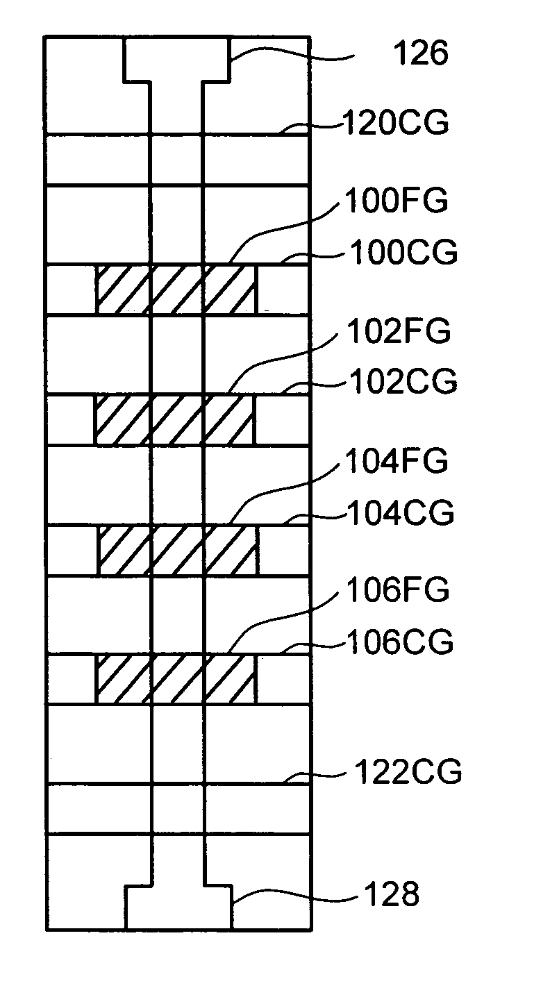
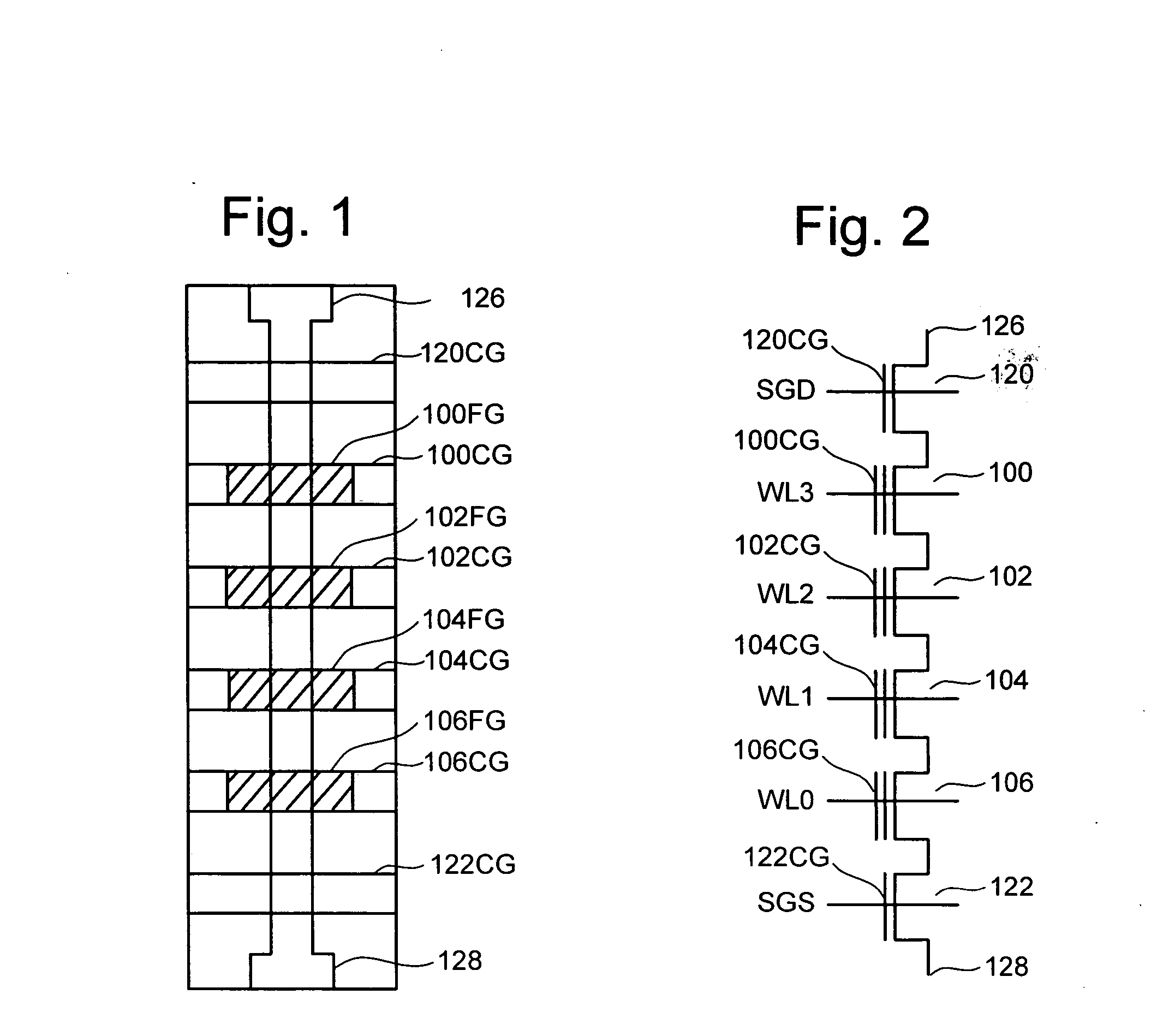
[0025]FIG. 1 is a top view showing one NAND string. FIG. 2 is an equivalent circuit thereof. Trench isolation techniques in accordance with embodiments are presented with respect to nonvolatile flash memory and NAND type memory for purposes of explanation. It will be appreciated by those of oridinary skill in the art, however, that the techniques set forth are not so limited and can be utilized in many fabrication processes to fabricate various types of integrated circuits.

[0026] The NAND string depicted in FIGS. 1 and 2 includes four transistors 100, 102, 104 and 106 in series and sandwiched between a first select gate 120 and a second select gate 122. Select gate 120 connects the NAND string to bit line 126. Select gate 122 connects the NAND string to source line 128. Each of the transistors 100, 102, 104 and 106 includes a control gate and a floating gate. For example, transistor 100 has control gate 100CG and floating gate 100FG. Transistor 102 includes control gate 102CG and a...


PUM


Abstract

Self-aligned trench filling to isolate active regions in high-density integrated circuits is provided. A deep, narrow trench is etched into a substrate between active regions. The trench is filled by growing a suitable dielectric such as silicon dioxide. The oxide grows from the substrate to fill the trench and into the substrate to provide an oxide of greater width and depth than the trench. Storage elements for a NAND type flash memory system, for example, can be fabricated by etching the substrate to form the trench after or as part of etching to form NAND string active areas. This can ensure alignment of the NAND string active areas between isolation trenches. Because the dielectric growth process is self-limiting, an open area resulting from the etching process can be maintained between the active areas. A subsequently formed inter-gate dielectric layer and control gate layer can fill the open area to provide sidewall coupling between control gates and floating gates.

Description

BACKGROUND OF THE INVENTION [0001] 1. Field of the Invention [0002] Embodiments of the present invention are directed to high density semiconductor devices, such as nonvolatile memory, and systems and methods for isolating active regions and components in high density semiconductor devices. [0003] 2. Description of the Related Art [0004] Integrated circuits are constructed by electrically connecting multiple isolated devices that share a common substrate. When multiple devices are formed on or in a common substrate, it is necessary to isolate the individual devices using isolation technology. As the density of integrated circuits continues to increase, the space available for isolating devices tends to decrease. With decreased device dimensions, inter-device parasitic currents and charges can become more problematic, making isolation technology a critical component of integrated circuit fabrication. [0005] For example, in nonvolatile semiconductor memory devices such as flash memory...

Claims


Application Information

Patent Timeline
Patent Type & Authority Applications(United States)
IPC IPC(8): H01L21/336
CPCH01L27/115H01L27/11521H10B69/00H10B41/30H01L21/28141H01L21/76224H01L21/76838
Inventor YUAN, JACK H.
Owner SANDISK TECH LLC
Why Eureka
Try Eureka