Method of forming a gate of a semiconductor device

a technology of semiconductor devices and gate oxides, applied in the field of semiconductor devices, can solve the problems of gate oxide layers having a greater thickness than desired, etching damage may be generated at surface portions of substrates, and the structure of semiconductor devices is complicated and multi-layered, so as to achieve the effect of improving the yield of semiconductor devices

Active Publication Date: 2006-05-25
SAMSUNG ELECTRONICS CO LTD
View PDF5 Cites 56 Cited by
  • Summary
  • Abstract
  • Description
  • Claims
  • Application Information

AI Technical Summary

Benefits of technology

[0014] Embodiments of the present invention provide a method of forming a gate for a semiconductor device that is capable of suppressing a punch-through and a short between wirings.
[0017] According to embodiments of the present invention, since whiskers that are generated in the oxidation process are reduced to the tungsten, generation of the whiskers due to a subsequent heat budget may be suppressed. Thus, a short between adjacent wirings may not be generated so that a yield of a semiconductor device may be improved. Further, since the oxygen radicals are used in the oxidation process, a punch-through phenomenon of the gate oxide layer may be suppressed.

Problems solved by technology

Semiconductor devices have become complicated multi-layered structures.
However, when the etching process is performed, etching damage may be generated at surface portions of the substrate, the polysilicon layer pattern and the tungsten layer pattern due to plasma used in the etching process.
On the contrary, a gate oxide layer may have a greater thickness than desired due to an excessive bird's beak.
The punch-through phenomenon may cause variable threshold voltage of a transistor or deteriorating reliability of the gate oxide layer.
Although the radical oxidation process may improve the punch-through phenomenon of the gate oxide layer, efficiency for curing the etching damage may be reduced and the gate electrode may not have a sufficiently rounded edge.
However, it is very difficult to prevent the oxidation of tungsten in the gate electrode.
As a result, a semiconductor device incorporating the gate electrode may operate abnormally.

Method used


Image

  • Method of forming a gate of a semiconductor device
  • Method of forming a gate of a semiconductor device
  • Method of forming a gate of a semiconductor device

Examples


embodiment 1

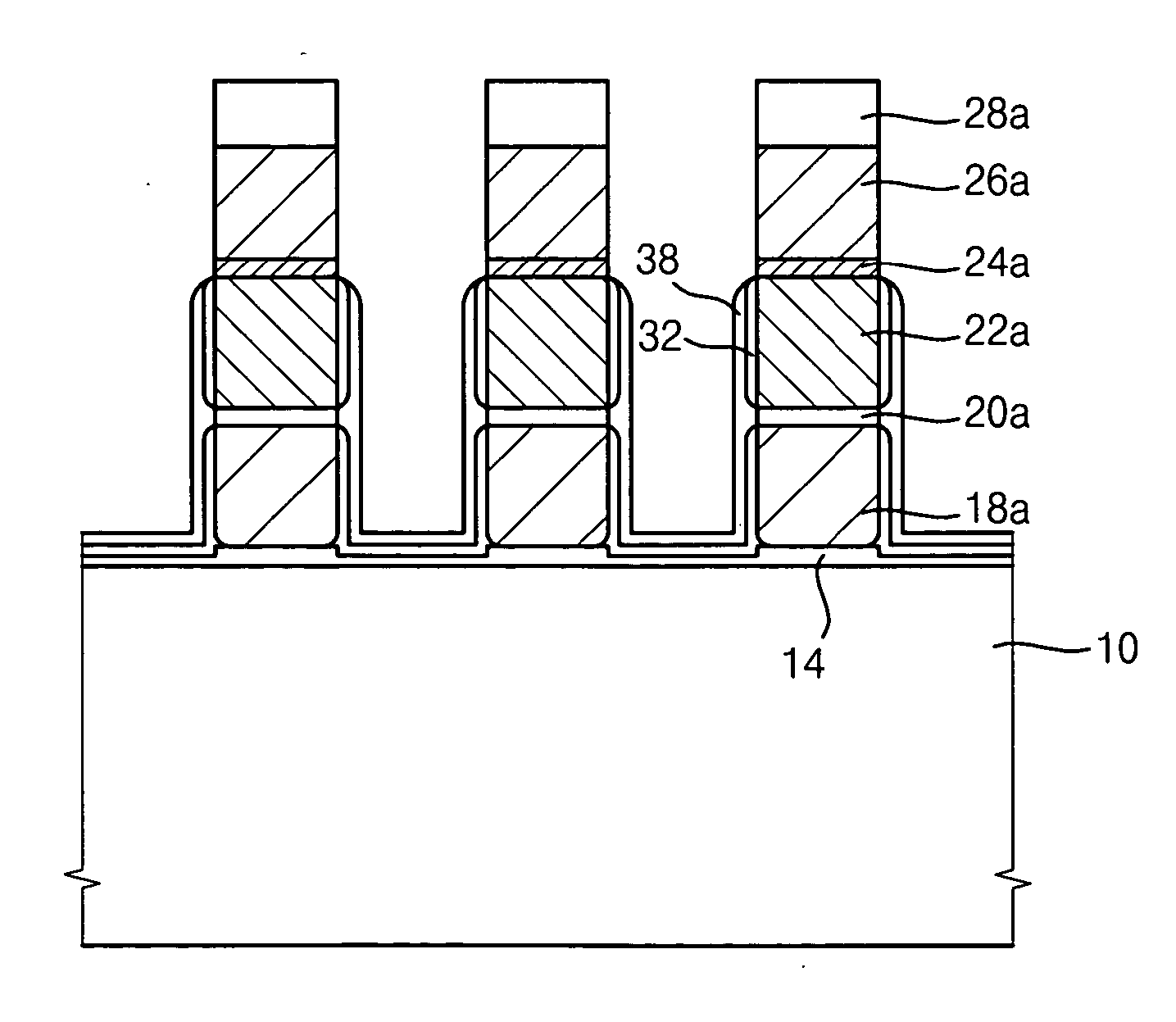
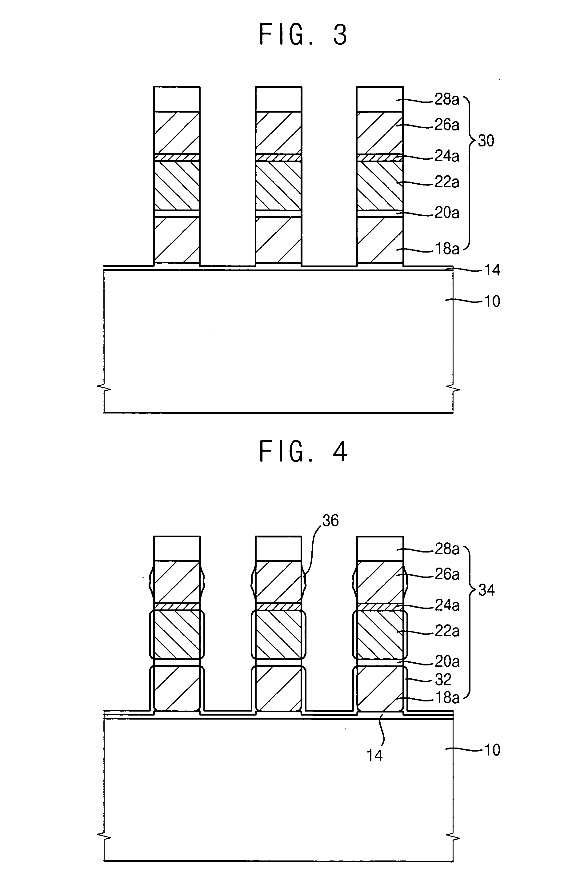
[0033] FIGS. 1 to 6 are cross sectional views illustrating a method of manufacturing a non-volatile memory device in accordance with a first exemplary embodiment of the present invention.

[0034] Referring to FIG. 1, an isolation region (not shown) of a silicon substrate 10 is selectively etched to form an isolation trench at a surface portion of the silicon substrate 10. Then, an insulation layer is formed in the trench and on the silicon substrate 10. The insulation layer is polished by a chemical mechanical polishing (CMP) process to form an isolation pattern (not shown) in the trench. An active region and the isolation region of the silicon substrate 10 are defined by the CMP process.

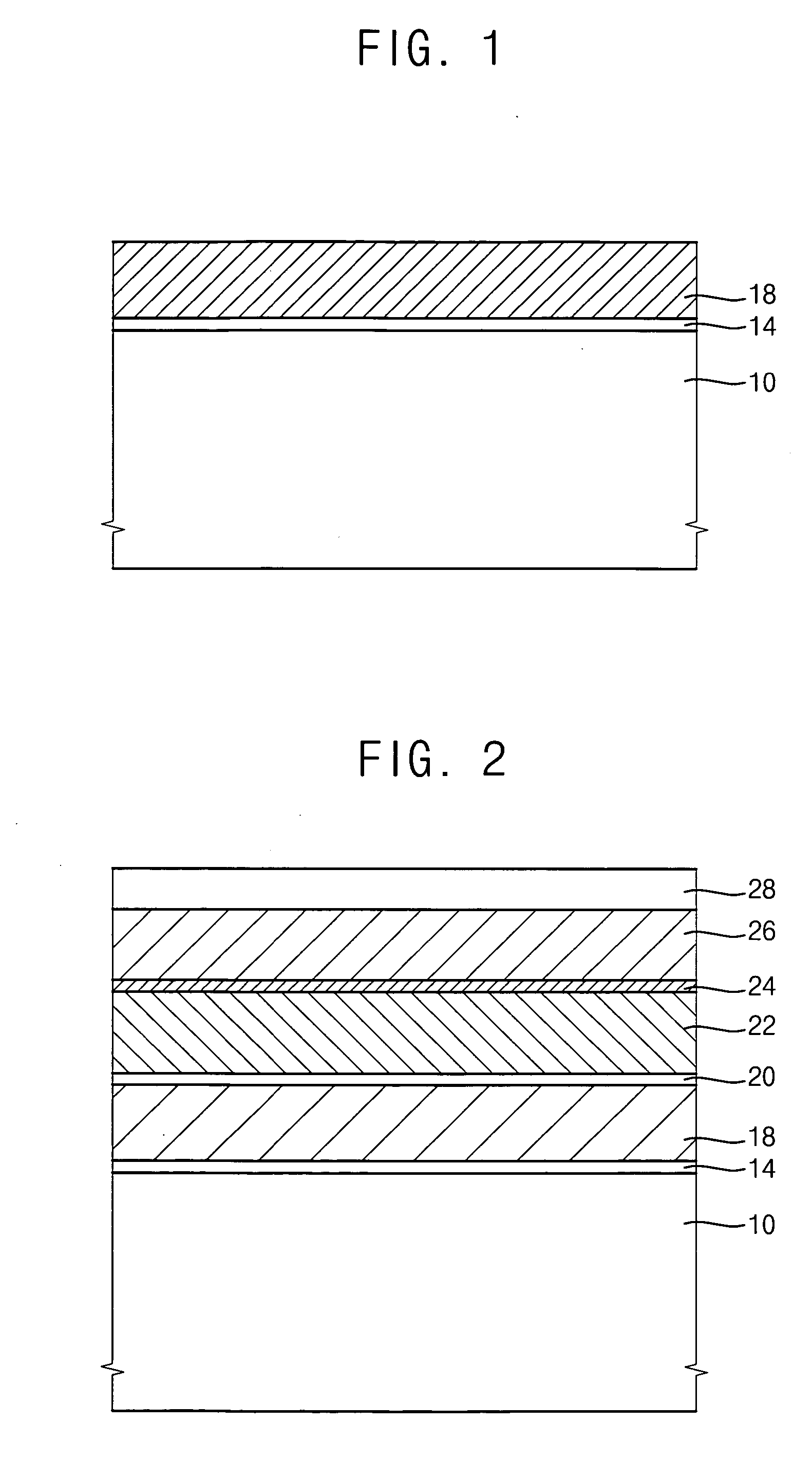
[0035] A tunnel oxide layer 14 is grown from exposed portions of the silicon substrate 10, which are the active region.

[0036] A first polysilicon layer (not shown) doped with impurities is formed on the tunnel oxide layer 14. The first polysilicon layer is used as a floating gate electrode by a sub...

embodiment 2

[0072] A method of forming a non-volatile memory device in Embodiment 2 is substantially identical to that in Embodiment 1 except for performing a hydrogen reduction process in a separate chamber. Thus, an oxidation process and the hydrogen reduction process are predominantly illustrated.

[0073] Processes substantially identical to those illustrated with reference to FIGS. 1 to 3 are carried out to form a first preliminary gate structure on a semiconductor substrate.

[0074] The oxidation process using oxygen radicals is then performed in a first chamber to convert the first preliminary gate structure into a second preliminary gate structure. The semiconductor substrate is loaded into a second chamber 56 with vacuum being continuously provided. The hydrogen reduction process is then carried out in the second chamber 56.

[0075]FIG. 10 is a flow chart illustrating a primary oxidation process and a hydrogen reduction process in accordance with the second exemplary embodiment of the pres...

embodiment 3

[0092]FIGS. 12 and 13 are cross sectional views illustrating a method of manufacturing a field effect transistor in accordance with Embodiment 3 of the present invention.

[0093] Referring to FIG. 12, an isolation layer 102 is formed in a trench of a silicon substrate 100 by a trench isolation process to define an active region and a field region of the semiconductor substrate 100. An exposed portion of the silicon substrate 100 is thermally treated to form a gate oxide layer on the active region.

[0094] A polysilicon layer doped with N-type impurities or P-type impurities is formed on the gate oxide layer 104. In this embodiment, the polysilicon layer is utilized as a gate electrode. Particularly, when an N-type transistor is to be formed, the polysilicon layer doped with N-type impurities is formed on the gate oxide layer 104. On the contrary, when a P-type transistor is to be formed, the polysilicon layer doped with P-type impurities is formed on the gate oxide layer 104. In a dyn...


PUM

PropertyMeasurementUnit
temperatureaaaaaaaaaa

Abstract

In a method for forming a gate in a semiconductor device, a first preliminary gate structure is formed on a substrate. The first preliminary gate structure includes a gate oxide layer, a polysilicon layer pattern and a tungsten layer pattern sequentially stacked on the substrate. A primary oxidation process is performed using oxygen radicals at a first temperature for adjusting a thickness of the gate oxide layer to form a second preliminary gate structure having tungsten oxide. The tungsten oxide is reduced to a tungsten material using a gas containing hydrogen to form a gate structure. The tungsten oxide may not be formed on the gate structure so that generation of the whiskers may be suppressed. Thus, a short between adjacent wirings may not be generated.

Description

CROSS REFERENCE TO RELATED APPLICATIONS [0001] This application claims priority under 35 USC § 119 to Korean Patent Application No. 2004-94894, filed on Nov. 19, 2004, the contents of which are herein incorporated by reference in its entirety. FIELD OF THE INVENTION [0002] The present invention relates generally to semiconductors and, more particularly, to semiconductor gates. BACKGROUND OF THE INVENTION [0003] Semiconductor devices have become complicated multi-layered structures. Further, semiconductor devices have become highly integrated. Thus, reducing the electrical resistance of conductive patterns such as gate electrodes has become desirable. [0004] Generally, a polysilicon layer pattern is employed in a gate electrode. To decrease electrical resistance of a gate electrode, a metal silicide layer pattern is formed on the polysilicon layer pattern. To reduce the electrical resistance of a gate electrode, a tungsten layer pattern is conventionally formed on the polysilicon lay...

Claims


Application Information

Patent Timeline
Patent Type & Authority Applications(United States)
IPC IPC(8): H01L21/4763
CPCH01L21/28044H01L21/28247H01L29/4925H01L21/18
Inventor YOUN, SUN-PILLEE, CHANG-WONSOHN, WOONG-HEECHOI, GIL-HEYUNYOO, JONG-RYEOLLEE, JANG-HEEPARK, JAE-HWALIM, DONG-CHANLEE, BYUNG-HAKPARK, HEE-SOOK
Owner SAMSUNG ELECTRONICS CO LTD
Why Eureka
Try Eureka