Multi-junction solar cells and methods of making same using layer transfer and bonding techniques

Active Publication Date: 2006-06-01
KONINKLIJKE PHILIPS ELECTRONICS NV
View PDF48 Cites 221 Cited by
  • Summary
  • Abstract
  • Description
  • Claims
  • Application Information

AI Technical Summary

Problems solved by technology

This design constraint along with materials integration limitations due to crystal lattice-matching requirements that accompany the use of epitaxy to fabricate multi-junction solar cells limit the number of subcells that can presently be integrated.

Method used


Image

  • Multi-junction solar cells and methods of making same using layer transfer and bonding techniques
  • Multi-junction solar cells and methods of making same using layer transfer and bonding techniques
  • Multi-junction solar cells and methods of making same using layer transfer and bonding techniques

Examples


first embodiment

ells Based on Active Si Sub-Cells

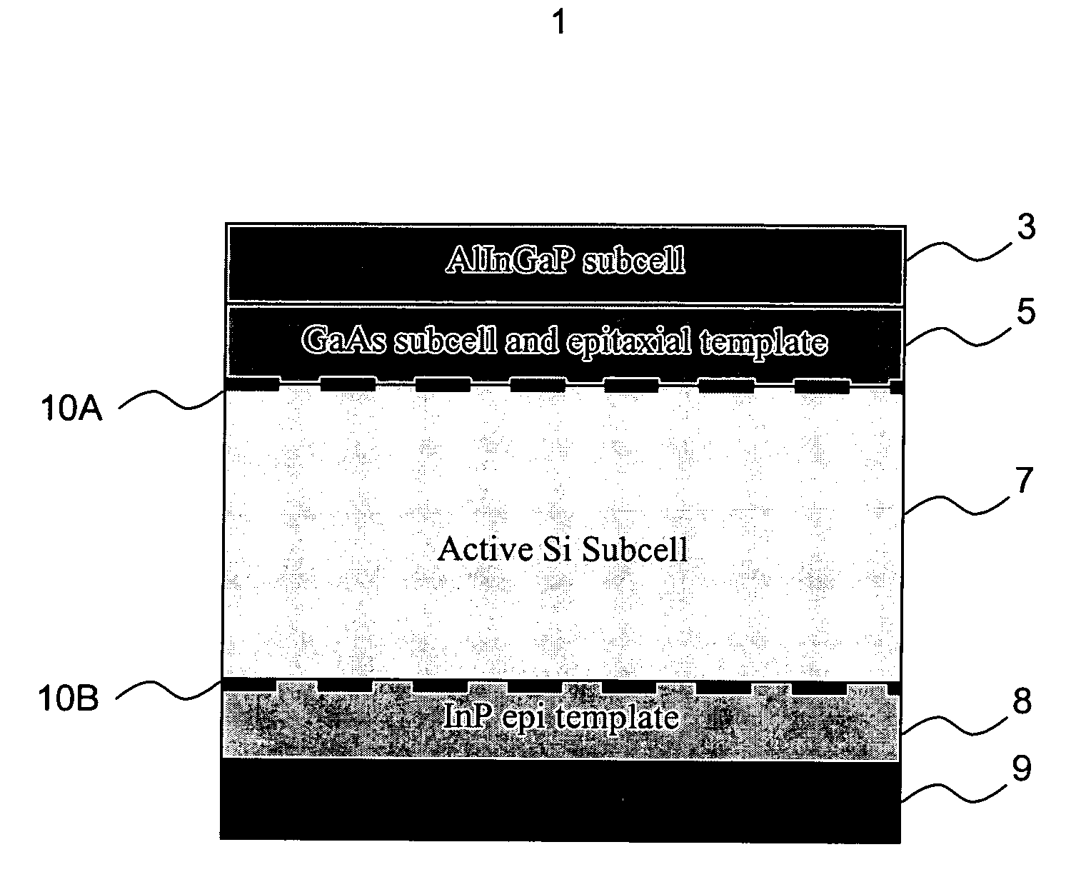
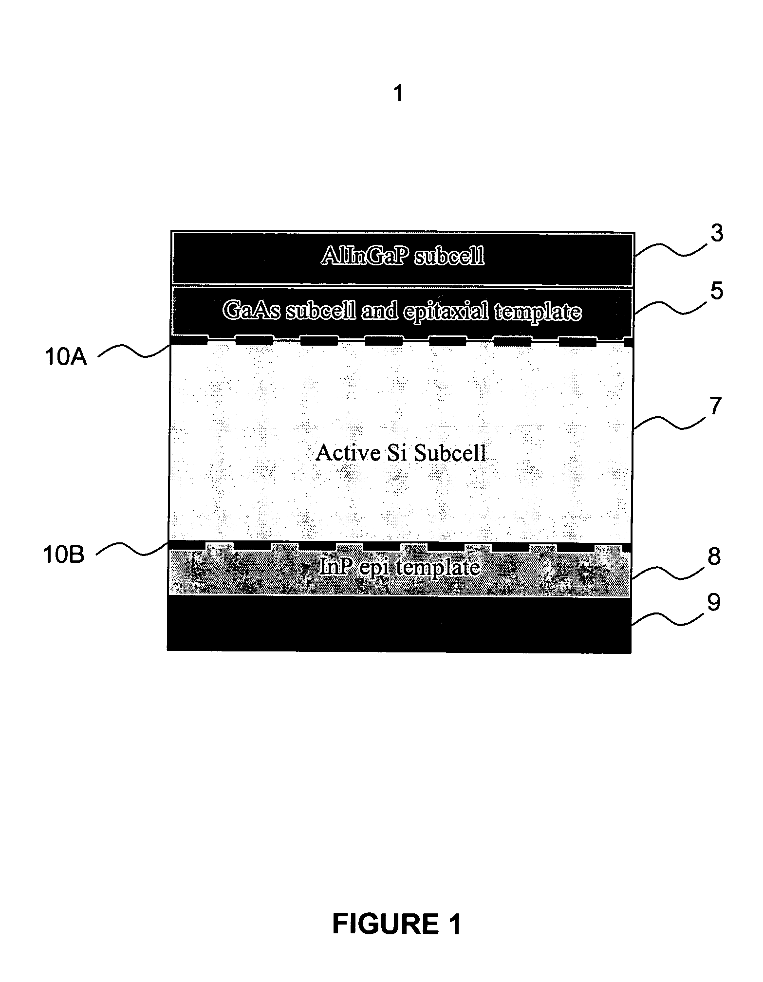
[0011] In the first embodiment of the invention, a multi-junction solar cell comprises an active silicon subcell, a first non-silicon subcell bonded to a first side of the active silicon subcell and a second non-silicon subcell bonded to a second side of the active silicon subcell. The first subcell comprises a p-n junction in a first non-silicon semiconductor material and the second subcell comprises a p-n junction in a second non-silicon semiconductor material different from the first semiconductor material. Preferably, the active silicon subcell comprises a silicon wafer containing a p-n junction. This forms a triple-junction solar cell in which the silicon subcell comprises a middle subcell with the other two non-silicon subcells being bonded to opposite sides of the silicon subcell.

[0012] If a four junction solar cell is desirable, then the solar cell further comprises a third non-silicon subcell comprising a p-n junction in a third non-silicon...

second embodiment

e

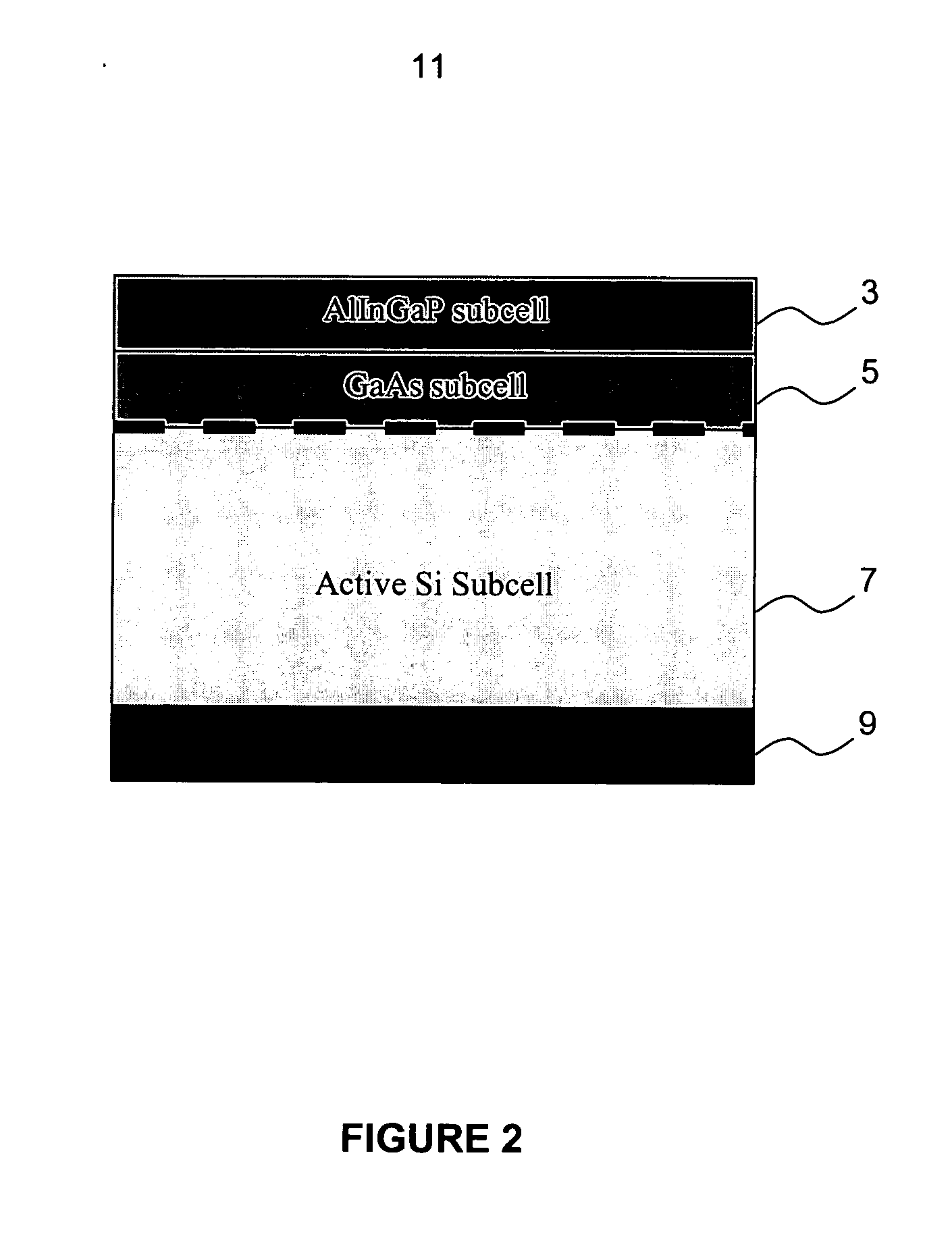
[0026] In a second embodiment of the invention, wafer bonding enables high-performance III-V and group IV solar cells to be bonded to flexible substrates. FIGS. 5 and 6 show two exemplary configurations for such a cell on a flexible substrate. In FIG. 5, a solar cell 41 comprised of AlInGaP and GaAs p-n junction subcells 3, 5 is bonded to a metallic bonding layer 43 that also serves as a backside electrical contact for the solar cell 41. The metal bonding layer 43 is formed over a flexible substrate, such as a flexible polymer substrate 45. A bonded interface 10 is located between subcell 5 and the metal layer 43.

[0027]FIG. 6 shows another exemplary solar cell 51. In this case, the subcells 3, 5 are directly bonded to a flexible, electrically-conductive polymer substrate 55. In this case, the metal layer 43 may be omitted because the polymer substrate is conductive and acts as a backside electrical contact. If the conductive substrate 55 is optically transparent, then it can act a...

third embodiment

Structure

[0029] The solar cells described herein may be made using an intermediate or temporary handle structure during fabrication. For example, one handle structure comprises a thin semiconductor film or layer that acts as an epitaxial template that has been bonded to an inexpensive handle substrate.

[0030] An intermediate handle structure is generally used herein to refer to a low-cost mechanical handle substrate that supports a thin transferred layer of semiconductor material. That semiconductor material then serves as an epitaxial template for the growth of a solar cell device structure. The design of the handle structure is such that following the fabrication of a solar cell device on the handle structure, the solar cell can be bonded to a secondary substrate or support, such as a Si substrate or a flexible film, as described in the first two embodiments. The handle substrate may comprise a semiconductor substrate or wafer, or a glass, plastic, metal or ceramic substrate. Upon...


PUM


Abstract

A multi-junction solar cell includes an active silicon subcell, a first non-silicon subcell bonded to a first side of the active silicon subcell, and a second non-silicon subcell bonded to a second side of the active silicon subcell. This and other solar cells may be formed by bonding and layer transfer.

Description

CROSS-REFERENCE TO RELATED PATENT APPLICATIONS [0001] The present application claims benefit of priority of U.S. provisional application Ser. No. 60 / 620,425, filed on Oct. 21, 2004, which is incorporated herein by reference it its entirety.BACKGROUND OF THE INVENTION [0002] The invention is directed to solar cells, such as multi-junction solar cells made by wafer bonding and layer transfer. [0003] There is considerable interest in the design and fabrication of tandem multi-junction solar cells for high efficiency photovoltaics for space-based and terrestrial applications. Multi-junction solar cells consist of two or more p-n junction subcells with band gaps engineered to enable efficient collection of the broad solar spectrum. The subcell band gaps are controlled such that as the incident solar spectrum passes down through the multi-junction solar cell it passes through subcells of sequentially decreasing band gap energy. Thus, the efficiency losses associated with single-junction c...

Claims


Application Information

Patent Timeline
Patent Type & Authority Applications(United States)
IPC IPC(8): H01L31/00
CPCH01L31/0687H01L31/06875H01L31/18Y02E10/544Y02P70/50
Inventor ATWATER, HARRY A. JR.ZAHLER, JAMESMORRAL, ANNA FONTCUBERTA IOLSON, SEAN
Owner KONINKLIJKE PHILIPS ELECTRONICS NV
Why Eureka
Try Eureka