Plating apparatus

a technology of plating apparatus and plating plate, which is applied in the direction of coating, manufacturing tools, liquid/solution decomposition chemical coating, etc., can solve the problems of high difficulty of conventional plating apparatus in producing a metal film that meets the requirements of such highly accurate uniformity, and failure of plating, etc., to achieve simple arrangement, increase the plating speed, and improve the effect of uniform thickness

Inactive Publication Date: 2006-06-01
EBARA CORP
View PDF9 Cites 34 Cited by
  • Summary
  • Abstract
  • Description
  • Claims
  • Application Information

AI Technical Summary

Benefits of technology

[0018] The present invention has been made in view of the above drawback. It is, therefore, a first object of the present invention to provide a plating apparatus which is capable of increasing the plating speed and adjusting flows of a plating solution more uniformly in a plating tank to achieve higher within-wafer uniformity of the film thickness of a plated film with a relatively simple arrangement.

Problems solved by technology

While highly dense packaging technologies such as SOC, WL-CSP, etc. available in recent years require more highly accurate uniformity, it would be highly difficult for the conventional plating apparatus to produce a metal film that meets the requirements for such highly accurate uniformity.
However, simply increasing the current density would cause burnt deposits, plating defects, passivation of the anode surface, etc., possibly resulting in plating failures.

Method used


Image

  • Plating apparatus
  • Plating apparatus
  • Plating apparatus

Examples


Embodiment Construction

[0088] Embodiments of the present invention will be described below with reference to the drawings. The following embodiments show examples in which a substrate such as a semiconductor wafer is used as a workpiece to be plated.

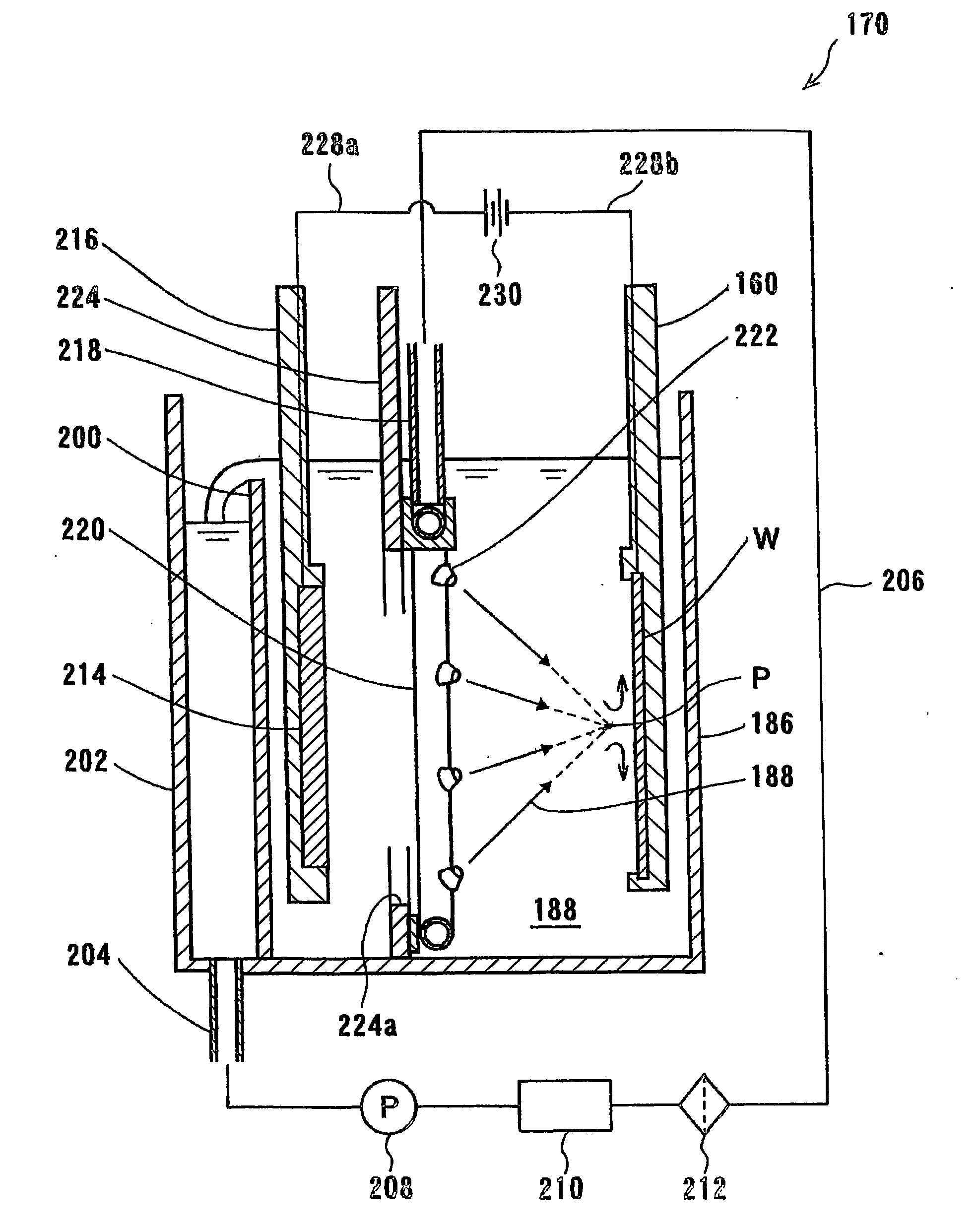
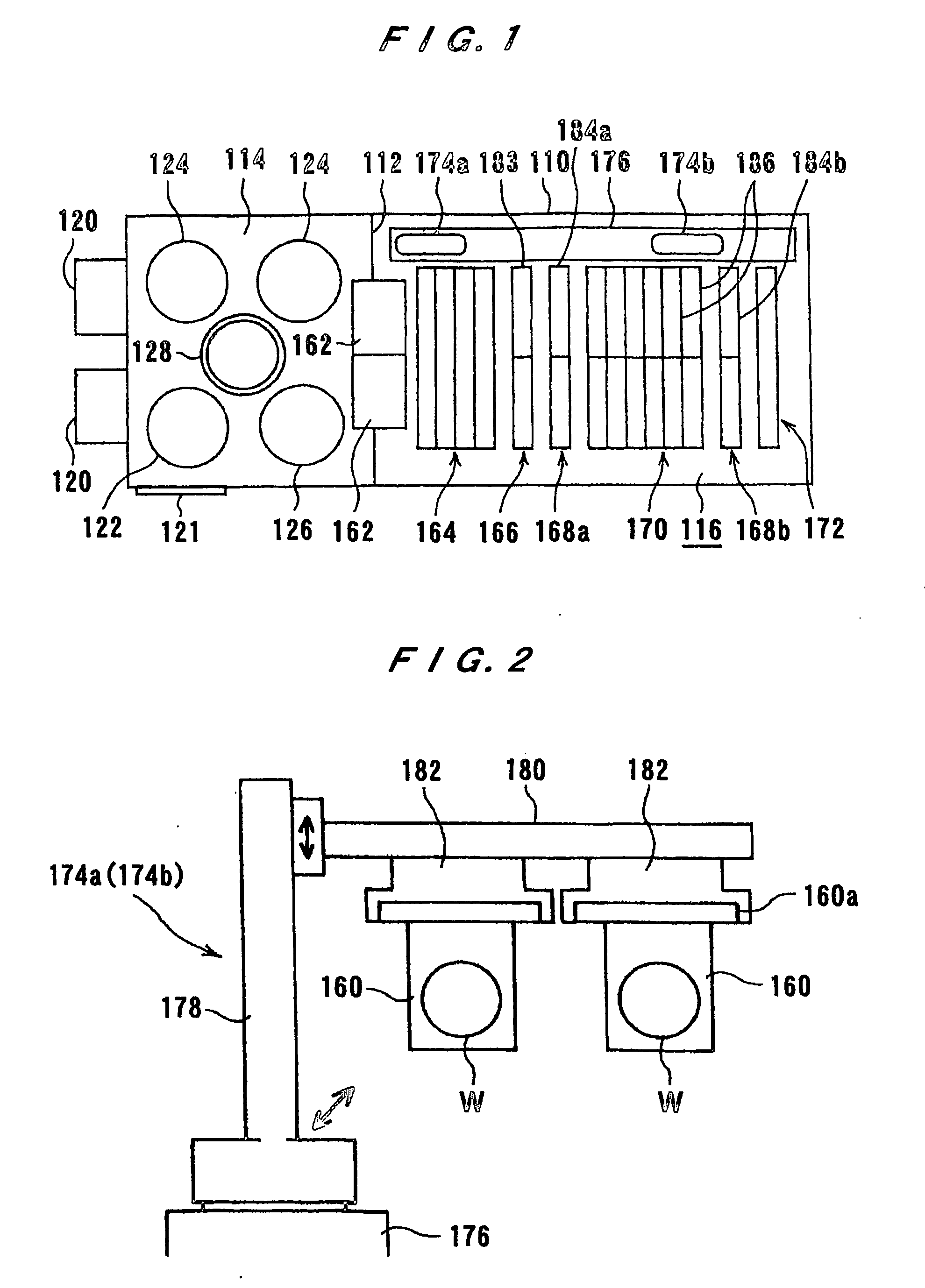
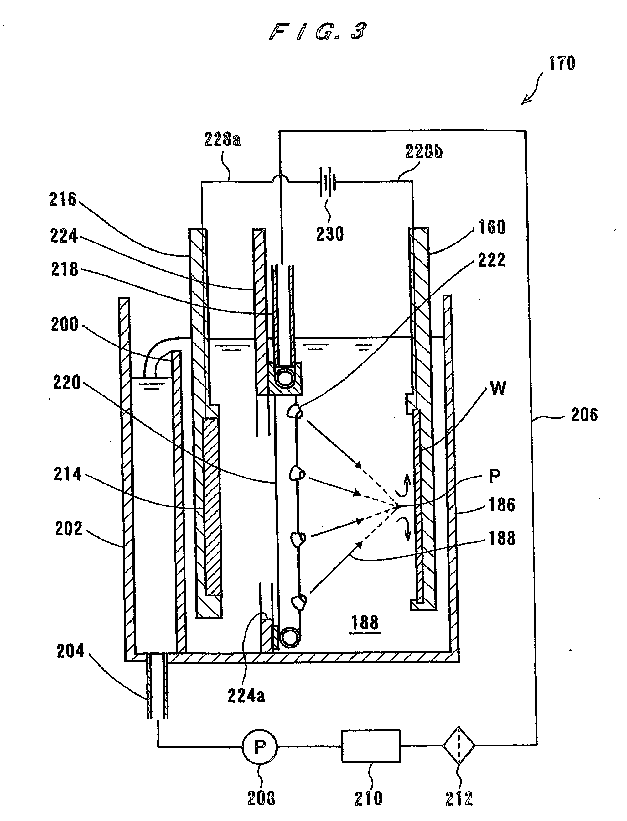
[0089]FIG. 1 shows an overall layout of a plating facility having a plating apparatus according to an embodiment of the present invention. The plating facility is designed so as to automatically perform all the plating processes including retreatment of a substrate, plating, and after treatment of the plating, in a successive manner. The interior of an apparatus frame 110 having an armored panel attached thereto is divided by a partition plate 112 into a plating space 116 for performing a plating process of a substrate and treatments of the substrate to which a plating solution is attached, and a clean space 114 for performing other processes, i.e. processes not directly involving a plating solution. Two substrate holders 160 (see FIG. 2) are arranged in para...


PUM

PropertyMeasurementUnit
heightaaaaaaaaaa
diameteraaaaaaaaaa
temperatureaaaaaaaaaa

Abstract

The present invention is concerned with a plating apparatus for use in forming a plated film in trenches, via holes, or resist openings that are defined in a surface of a semiconductor wafer, and forming bumps to be electrically connected to electrodes of a package, on a surface of a semiconductor wafer. The plating apparatus (170) has a plating tank (186) for holding a plating solution (188), a holder (160) for holding a workpiece (W) and bringing a surface to be plated of the workpiece into contact with the plating solution (188) in the plating tank (186), and a ring-shaped nozzle pipe (220) disposed in the plating tank (186) and having a plurality of plating solution injection nozzles (222) for injecting the plating solution (188) to the surface to be plated of the workpiece held by the holder (160) to supply the plating solution (188) into the plating tank (186).

Description

TECHNICAL FIELD [0001] The present invention relates to a plating apparatus for plating a surface (a surface to be plated) of a substrate or the like, and more particularly to a plating apparatus for use in forming a metal film and interconnects on a substrate for LSI circuits or the like according to plating technology, forming a plated film in fine interconnect grooves (trenches), via holes, or resist openings that are defined in a surface of a semiconductor wafer or the like, and forming bumps (protruding electrodes) to be electrically connected to electrodes of a package or the like, on a surface of a semiconductor wafer. BACKGROUND ART [0002] In recent years, there has been employed a method of forming interconnects or bumps in semiconductor circuits by forming metallic films on silicon wafers or other substrates according to plating technology. [0003] In TAB (Tape Automated Bonding) or FC (Flip Chip), for example, it has widely been practiced to form protruding connecting elec...

Claims


Application Information

Patent Timeline
Patent Type & Authority Applications(United States)
IPC IPC(8): C25B9/00C25C7/00C23C18/16C23C18/54C25D5/02C25D5/08C25D7/12C25D17/00C25D21/10H01L21/288H01L21/60
CPCC23C18/1628H01L2224/1147C25D21/10H01L21/288H01L21/2885H01L24/11H01L2224/13099H01L2924/01002H01L2924/01004H01L2924/01015H01L2924/01029H01L2924/01033H01L2924/01074H01L2924/01078H01L2924/01079H01L2924/01082H01L2924/01005H01L2924/01006H01L2924/01023H01L2924/01076H01L2924/014C25D17/008C25D7/123C25D17/001C25D5/08H01L2224/05568H01L2224/05573H01L2924/14H01L2924/00
Inventor KURIYAMA, FUMIOTAKEMURA, TAKASHISAITO, NOBUTOSHIKIMURA, MASAAKIKIUMI, REI
Owner EBARA CORP
Why Eureka
Try Eureka