Plating device and planting method

Inactive Publication Date: 2006-06-01
IBM CORP +1
View PDF9 Cites 23 Cited by
  • Summary
  • Abstract
  • Description
  • Claims
  • Application Information

AI Technical Summary

Benefits of technology

[0106] With this arrangement, the thickness of the metal film on the surface of the substrate is measured, and plating time is increased or decre

Problems solved by technology

If the amount of copper to be removed is larger, then CMP requires a longer period of time, thereby causing an increased cost.
Further, if a substrate has non-uniformity on its polished surface after CMP, then interconnects remaining after polishing have different depths over the surface of the substrate.
Thus, a longer period of polishing time increases a degree of dependence of interconnect performance upon CMP performance.
These ideas can achieve the object to a certain extent but have a limitation.
On the other hand, in a method comprising bringing a porous member into contact with a substrate and plating-the substrate while relatively moving the porous member in a contact direction, a porous member, which generally has a surface roughness in a range of from several micrometers to several hundred micrometers, is problematic to planarize projections and depressions on a semiconductor substrate having a surface roughness in a range of from submicrometers to several micrometers.
However, it is difficult to obtain expected results because of the surface roughness as described above.
Further, it is difficult to uniformly press the overall surface of the porous member against the surface, to be plated, of the substrate so as to bring it into close contact with the surface of the substrate because of the surface roughness of the

Method used


Image

  • Plating device and planting method
  • Plating device and planting method
  • Plating device and planting method

Examples


example

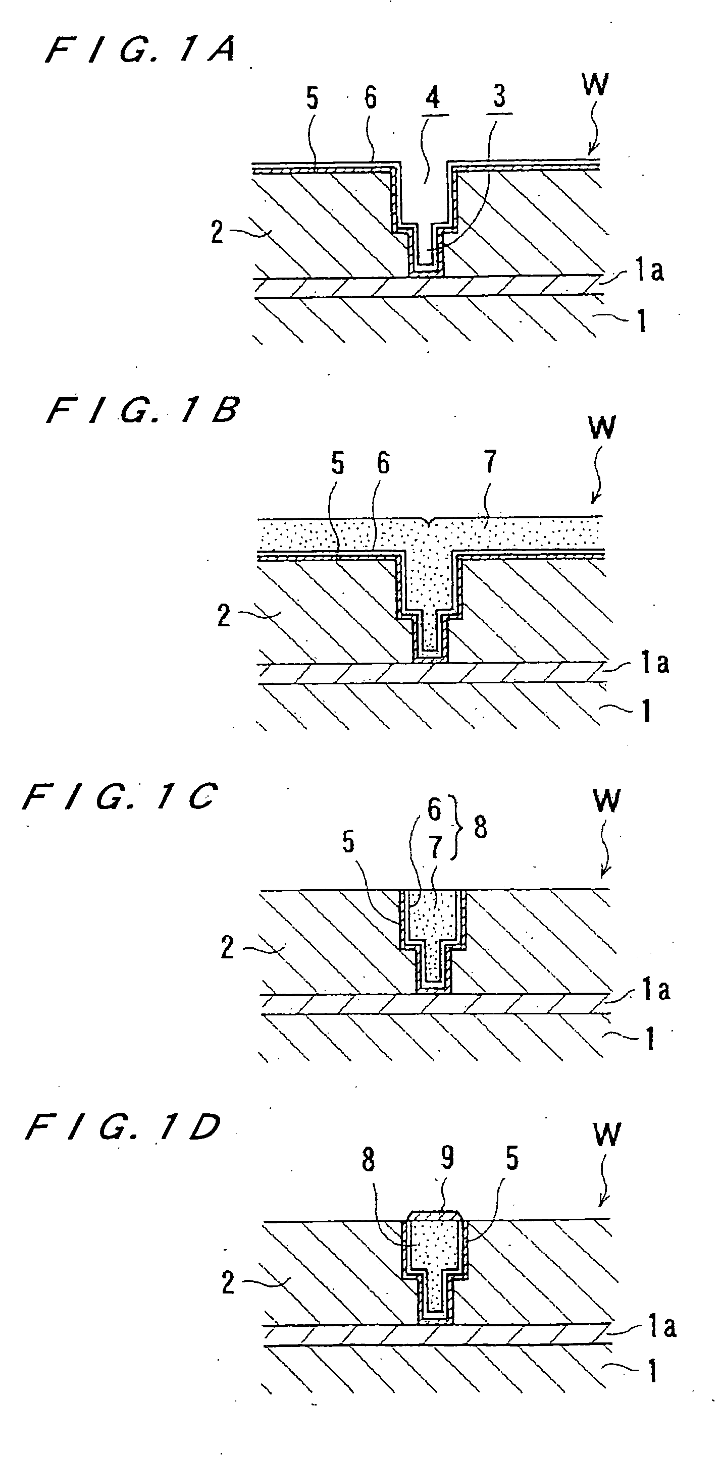
[0288] A barrier metal process was performed on the substrate W having narrow trenches (having a depth of 1 μm and a width of 0.18 μm) 4a and wide trenches (having a width of 100 μm) 4b having a larger width than the narrow trenches by a conventional method. Next, the seed layer 6 having a thickness of 80 nm was formed on the substrate W by sputtering, and then the substrate W was used as a testing sample.

[0289] This testing sample was plated using an acid copper plating solution having composition shown in Table 1 by a plating apparatus having the electrode head (the anode 704 is composed of copper containing phosphorus having holes) 701 having the structure shown in FIG. 34. The plating condition is shown in FIG. 36. As a current-flowing pattern, first, in a state that the porous contact member 702 was brought out of contact with the seed layer 6, plating was started at a plating voltage of 1V, and after an elapse of ten seconds, current supply was stopped. Thereafter, the porous...


PUM

PropertyMeasurementUnit
Temperatureaaaaaaaaaa
Thicknessaaaaaaaaaa
Pressureaaaaaaaaaa

Abstract

According to the present invention, there is provided a plating apparatus which can deposit a metal plated film such as a copper layer selectively in fine recesses for interconnects, such as trenches or via holes in a circuit form. The plating apparatus of the present invention includes an electrode head (701) having an anode (704), a plating solution impregnated material (703) for holding a plating solution, and a porous contact member (702) which is brought into contact with a surface of a substrate; a cathode electrode (712) which is brought into contact with the substrate to supply current to the substrate; a pressing mechanism (709) for pressing the porous contact member of the electrode head against the surface of the substrate under a desired pressure; a power source (723) for applying plating voltage between the anode and the cathode electrode; and a control unit (721) for correlating and controlling the state for pressing the porous contact member of the electrode head against the surface of the substrate, and the state of plating voltage applied between the anode and the cathode electrode.

Description

TECHNICAL FIELD [0001] The present invention relates to a plating apparatus and a plating method, and more particularly to a plating apparatus and a plating method used for filling a fine interconnect pattern formed in a substrate, such as a semiconductor substrate, with metal (interconnect material) such as copper so as to form interconnects. BACKGROUND ART [0002] Recently, there has been employed a circuit forming method comprising forming fine recesses for interconnects, such as trenches or via holes in a circuit form, in a semiconductor substrate, embedding the fine recesses with copper (interconnect material) by copper plating, and removing a copper layer (plated film) at portions other than the fine recesses by CMP means or the like. In this method, from the viewpoint of reducing loads on subsequent CMP, it is desirable that a copper plated film be deposited selectively in trenches or via holes in a circuit form, and that the amount of copper plated film deposited on portions ...

Claims


Application Information

Patent Timeline
IPC IPC(8): C25D21/12C25B9/00C25D5/06C25D7/12C25D17/00H01L21/288
CPCC25D5/06C25D7/12C25D17/00H01L21/2885C25D7/123C25D17/001C25D17/14C25D5/20C25D21/12H01L21/76879
Inventor KURASHINA, KEIICHINAMIKI, KEISUKENAKADA, TSUTOMUMISHIMA, KOJI
Owner IBM CORP
Why Eureka
Try Eureka