Printed circuit board and manufacturing method thereof

a technology of printed circuit board and manufacturing method, which is applied in the association of printed circuit non-printed electric components, metal working apparatus, and incorporation of printed electric components, etc. it can solve the problems of limited movement of metal ions eluted from the conductive layer and further limited movement of metal ions, so as to prevent ion migration of a conductor

Inactive Publication Date: 2006-06-01
NITTO DENKO CORP
View PDF19 Cites 8 Cited by
  • Summary
  • Abstract
  • Description
  • Claims
  • Application Information

AI Technical Summary

Benefits of technology

[0010] It is an object of the invention to provide a printed circuit board that can sufficiently prevent ion migration of a conductor in a high temperature and high humidity atmosphere and a manufacturing method thereof.

Problems solved by technology

In this way, in a high temperature and high humidity atmosphere, the movement of metal ions eluted from the conductive layer is limited by the irregularities on the insulating layer.
When another insulating layer is provided to cover the surface of the insulating layer having the conductive layer thereon, the adhesion between these insulating layers improves, and the movement of the metal ions is further limited.

Method used


Image

  • Printed circuit board and manufacturing method thereof
  • Printed circuit board and manufacturing method thereof
  • Printed circuit board and manufacturing method thereof

Examples


##ventive example 1

INVENTIVE EXAMPLE 1

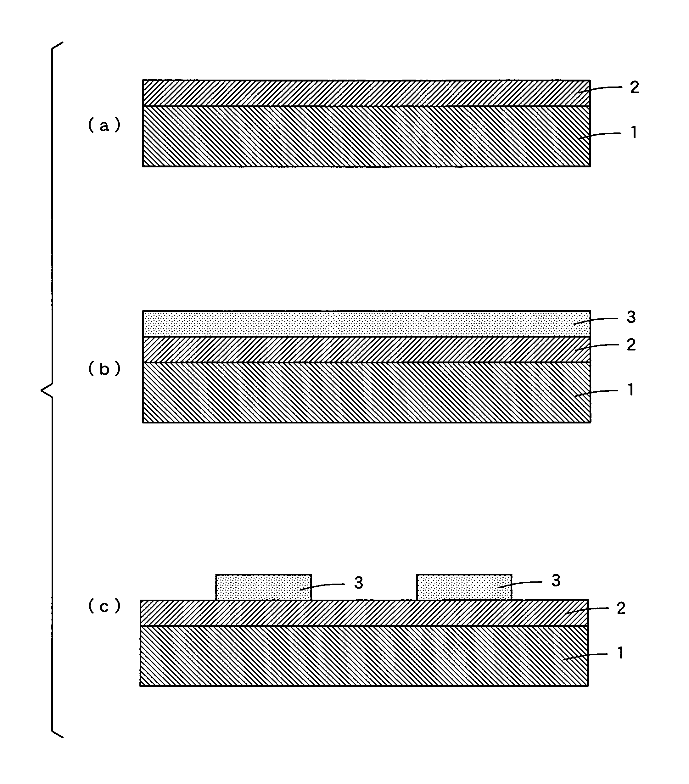
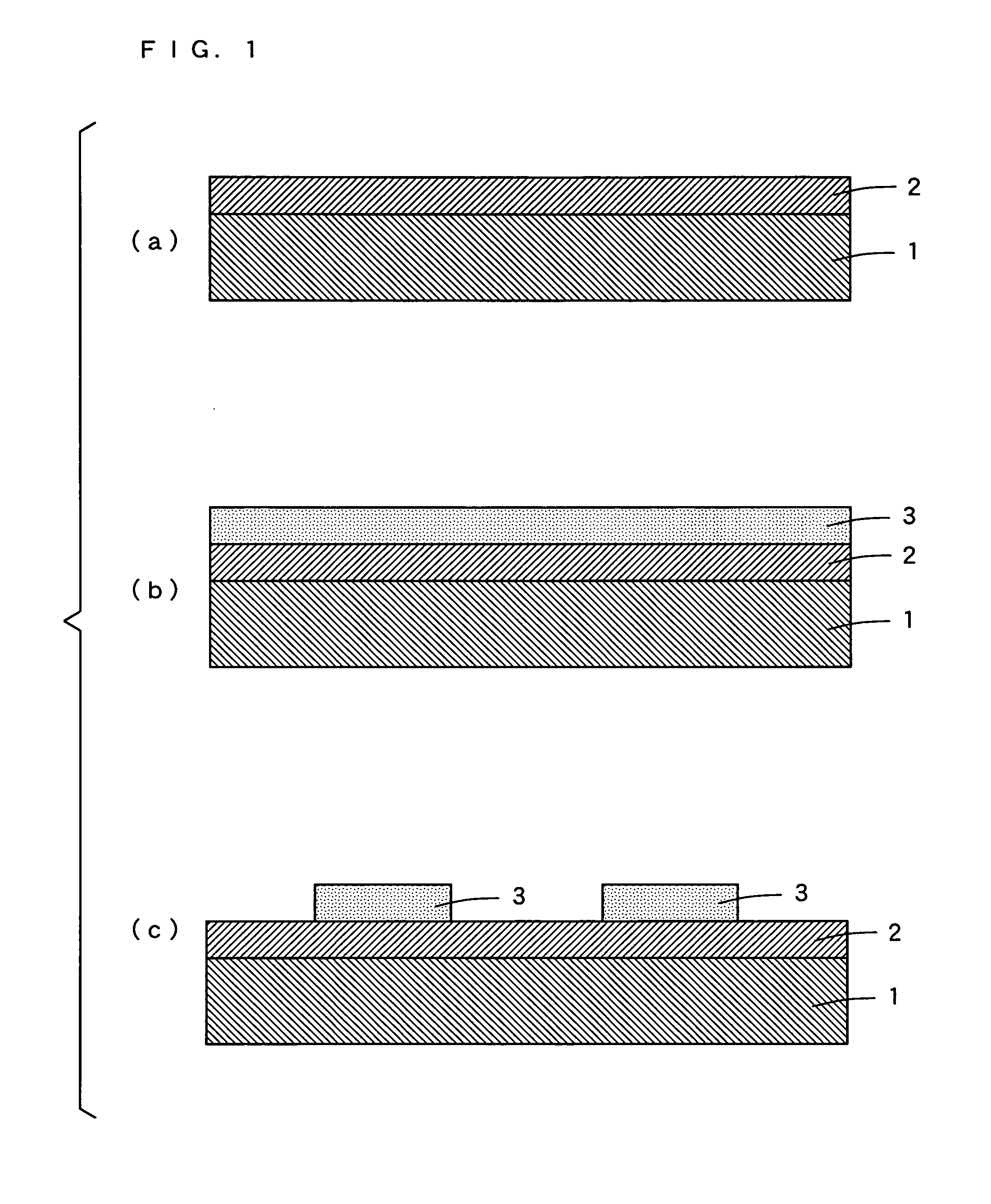
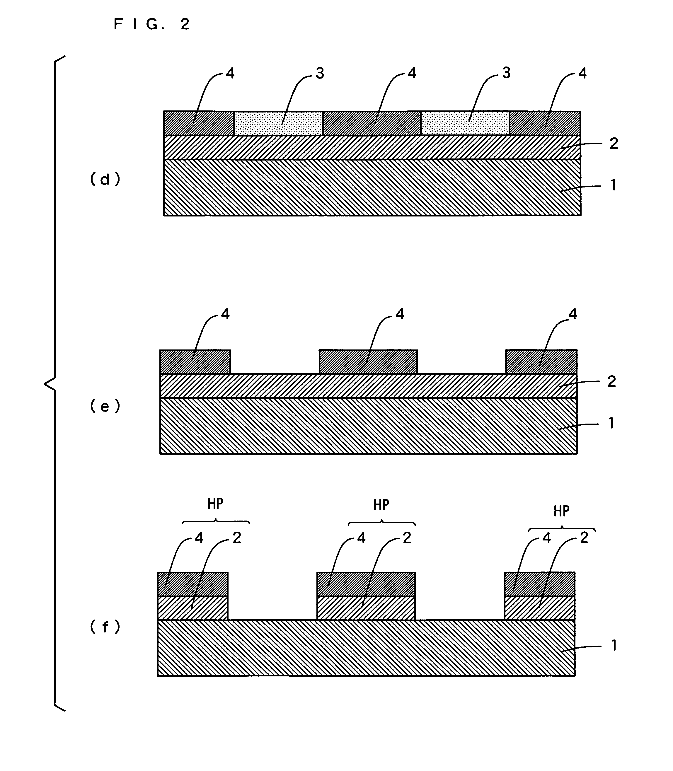
[0055] When the printed circuit board 10 according to Inventive Example 1 was produced, conductive patterns HP were formed according to the semi-additive method similarly to the above example, details of which will be described.

[0056] To start with, a polyimide resin film having a thickness of 25 μm was prepared as a base insulating layer 1. A sputtering film of nickel and a sputtering film of copper were formed as a thin metal film layer 2 on the upper surface of the base insulating layer 1 by continuous sputtering. In this case, the nickel sputtering layer had a thickness of 30 nm and the copper sputtering film had a thickness of 200 nm.

[0057] Then, a plating resist layer 3 made of photosensitive resin was formed on the upper surface of the thin metal film layer 2. Then, the plating resist layer 3 was subjected to exposure and development treatment using a prescribed pattern. In this way, the plating resist layer 3 having the prescribed pattern was formed on t...


PUM

PropertyMeasurementUnit
surface roughnessaaaaaaaaaa
thicknessaaaaaaaaaa
thicknessaaaaaaaaaa

Abstract

A multi-layer structure including a base insulating layer and a thin metal film layer (seed layer) is prepared. A plating resist layer is formed to have a prescribed pattern on the upper surface of the thin metal film layer. A metal plating layer is formed on the thin metal film layer exposed by electroplating. Then, the plating resist layer is removed, and the thin metal film layer in the region having the plating resist layer is removed. In this way, a conductive pattern including the thin metal film layer and the metal plating layer is formed. The upper surface of the base insulating layer in the region without the conductive pattern is subjected to roughening treatment. A cover insulating layer is formed on the upper surfaces of the base insulating layer and the conductive pattern. In this way, a printed circuit board is completed.

Description

BACKGROUND OF THE INVENTION [0001] 1. Field of the Invention [0002] The invention relates to a printed circuit board and a manufacturing method thereof. [0003] 2. Description of the Related Art [0004] As a method of manufacturing a printed circuit board, a subtractive method, an additive method, and a semi-additive method are known. [0005] For example, a printed circuit board is manufactured according to the subtractive method as follows (see Japanese Patent Laid-Open No. 2002-252257). To start with, a thin metal film is formed as an adhesion promoting layer (seed layer) by sputtering on a base insulating layer such as a polyimide film. Then, a metal plating layer is formed on the thin metal film. [0006] The metal plating layer is then coated with photoresist in a prescribed pattern, followed by drying, and then subjected to process of exposure, development, and etching. Then, the photoresist is removed and a complete conductive (interconnection) pattern forms. [0007] In another exa...

Claims


Application Information

Patent Timeline
Patent Type & Authority Applications(United States)
IPC IPC(8): H01L23/48H01L21/4763
CPCH05K1/0393Y10T29/49155H05K3/0041H05K3/108H05K3/22H05K3/281H05K3/381H05K3/386H05K3/388H05K2203/025H05K2203/095Y10T29/49165Y10T29/49117Y10T29/49128Y10T29/53504H05K3/002
Inventor OOKAWA, TADAOHONJO, MITSURUODA, TAKASHI
Owner NITTO DENKO CORP
Why Eureka
Try Eureka