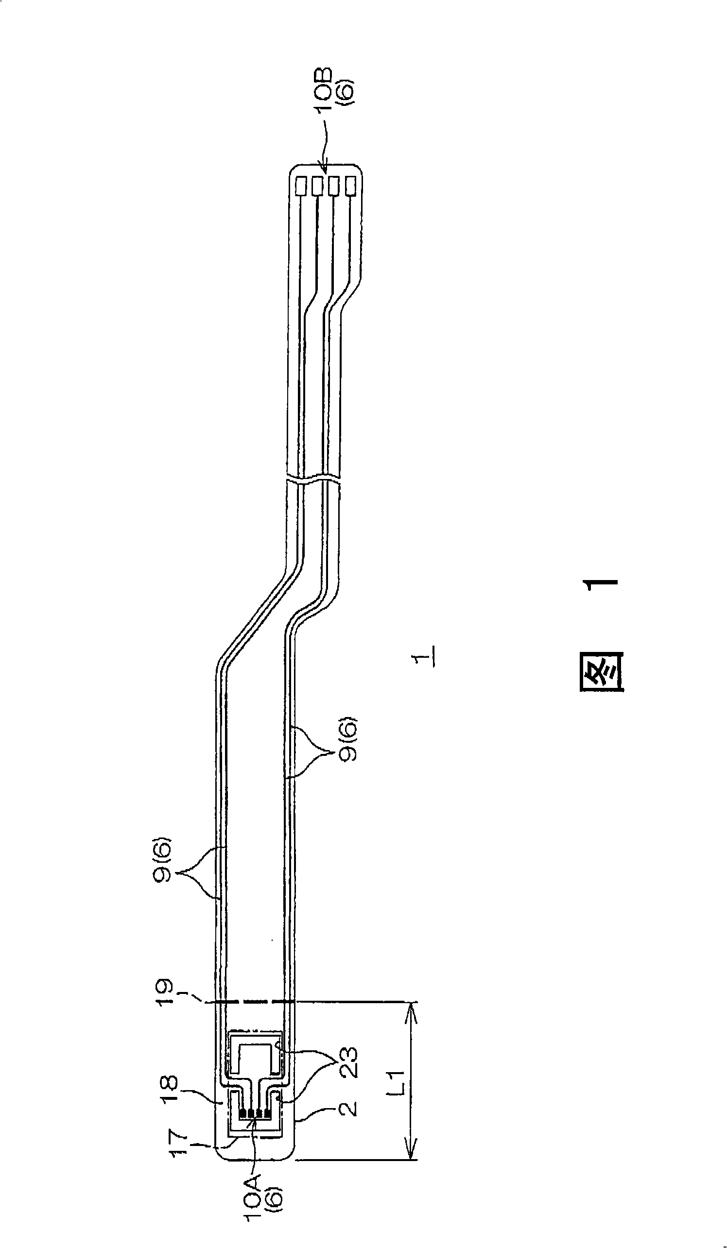
Wired circuit board

A technology for wiring circuit substrates and substrates, which is applied in the direction of circuit substrate materials, printed circuits, printed circuits, etc., can solve the problems of increased transmission loss of conductor patterns, prevent ion migration, reduce transmission loss, and improve shape retention. Effect

Inactive Publication Date: 2009-01-21
NITTO DENKO CORP
View PDF1 Cites 0 Cited by
  • Summary
  • Abstract
  • Description
  • Claims
  • Application Information

AI Technical Summary

Problems solved by technology

[0003] In this suspension board with circuit, since the metal supporting board is made of stainless steel, the transmission loss in the conductor pattern becomes large.

Method used


Image

  • Wired circuit board
  • Wired circuit board
  • Wired circuit board

Examples


Embodiment 1

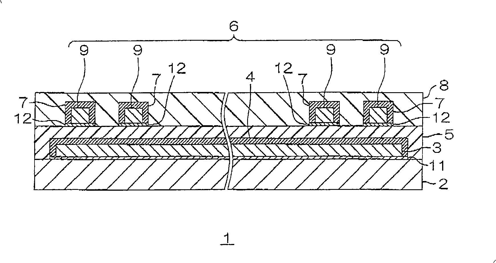
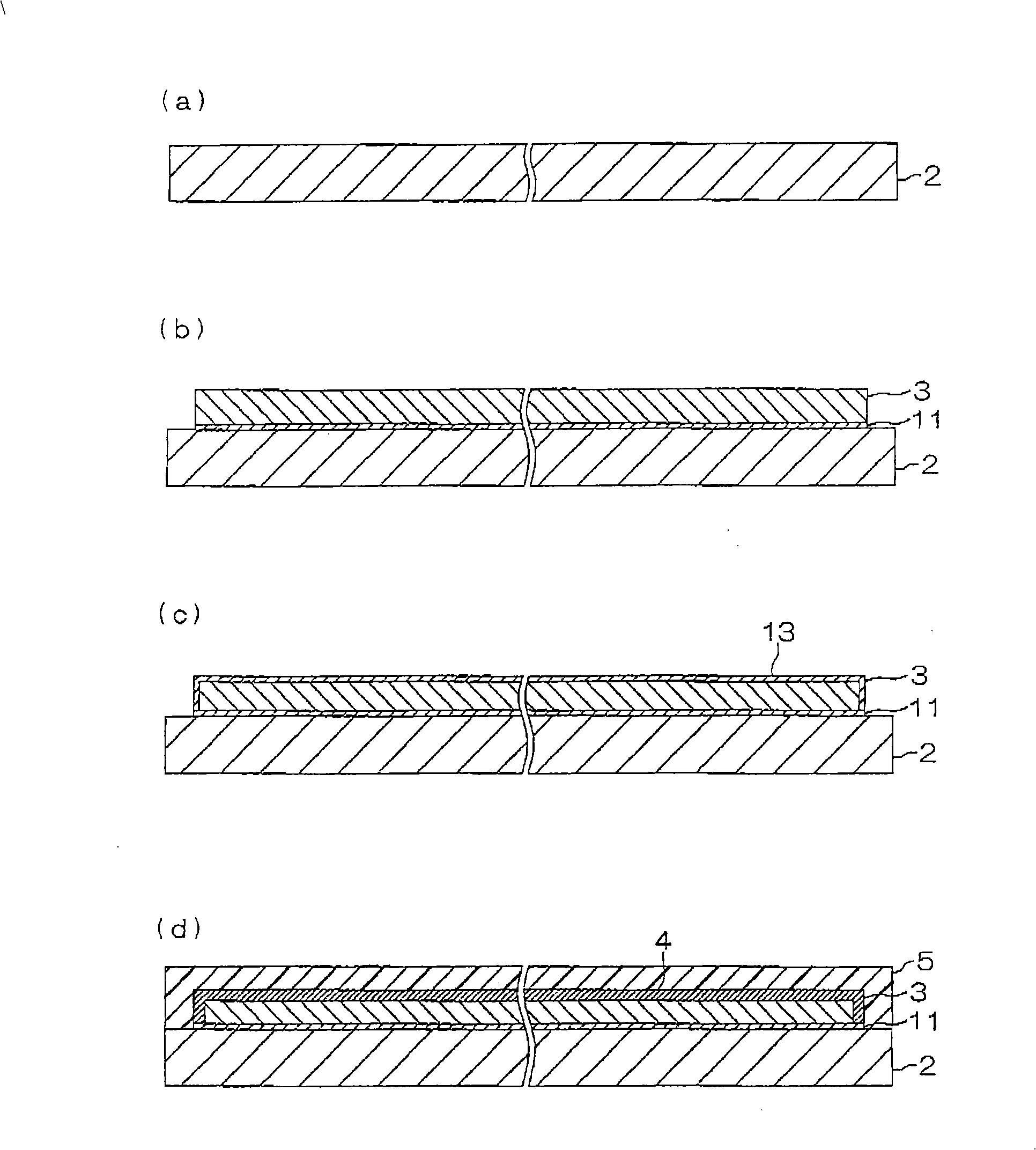
[0127] First, prepare a metal support substrate made of stainless steel with a thickness of 25 μm (see image 3 (a)) Next, a chromium thin film with a thickness of 50 nm and a copper thin film with a thickness of 100 nm were sequentially formed by sputtering on the entire surface of the metal supporting substrate to form a first metal thin film. Next, after forming a plating protection layer with a pattern opposite to that of the metal foil on the upper surface of the first metal thin film 11, a copper foil with a thickness of 3 μm is formed by electrolytic copper plating (refer to image 3 (b)). Then, form the first tin layer with a thickness of 0.4 μm by electroless tin plating on the upper surface of the copper foil, both sides in the width direction and both sides in the longitudinal direction (refer to image 3 (c)).

[0128] Then, a photosensitive polyamic acid varnish was applied to the entire upper surface of the metal supporting substrate including the first tin lay...

Embodiment 2

[0134] In addition to the 1st tin layer (refer to image 3 (c)) the thickness is changed to 0.3μm, the second tin layer (refer to Figure 4 Except that the thickness of (f)) was changed to 0.3 μm, the same operation as in Example 1 was performed to obtain a suspension board with circuit. The thickness of the first protective layer was 0.8 μm, and the thickness of the second protective layer was 0.8 μm.

Embodiment 3

[0136] Except that the lower base insulating layer is interposed between the metal thin film and the metal supporting substrate, the same operation is performed as in Example 1 to obtain a suspension board with circuit (refer to Figure 6 ).

[0137] That is, a varnish of photosensitive polyamic acid resin was applied to the entire surface of the metal supporting substrate, dried by heating at 90°C for 15 minutes, and cured by heating at 370°C for 120 minutes under reduced pressure after exposure and development. amination), thereby forming a lower base insulating layer with a thickness of 3 μm. Then, a chromium thin film with a thickness of 50 nm and a copper thin film with a thickness of 100 nm were sequentially formed by sputtering on the entire surface of the metal supporting substrate including the lower insulating base layer, thereby forming a first metal thin film.


PUM

PropertyMeasurementUnit
thicknessaaaaaaaaaa
thicknessaaaaaaaaaa
thicknessaaaaaaaaaa

Abstract

A wired circuit board comprises a metal supporting board, a metal foil formed on the metal supporting board, a first protecting layer formed on the surface of the metal foil, the first protecting layer is made of tin or a tin alloy, a first insulating layer formed on the metal supporting board to cover the first protecting layer, a conductive pattern formed on the insulating layer, and a second protecting layer formed on the surface of the conductive pattern, the second protecting layer is made of tin or a tin alloy.

Description

technical field [0001] The present invention relates to a wired circuit board, and more particularly to a wired circuit board usable as a suspension board with circuit. Background technique [0002] Conventionally, a suspension board with circuit is known in which an insulating layer made of resin and a conductive pattern made of copper are sequentially formed on a metal supporting board made of stainless steel, and a magnetic head is mounted thereon and used for a hard disk drive or the like. [0003] In this suspension board with circuit, since the metal supporting board is made of stainless steel, the transmission loss in the conductor pattern becomes large. Therefore, in order to reduce the transmission loss, a technique has been proposed in which a lower conductor made of copper or a copper alloy containing copper as a main component is formed on the suspension board, and an insulating layer, a recording-side conductor, and a regeneration-side conductor are sequentially...

Claims


Application Information

Patent Timeline
Patent Type & Authority Applications(China)
IPC IPC(8): H05K1/02H05K1/05H05K3/10
CPCH05K2201/057H05K2201/0338H05K1/028G11B5/486H05K3/244H05K1/0237H05K1/056H05K3/28H05K2203/302H05K2203/1105
Inventor 龟井胜利V·塔维普斯皮波恩中村和哉
Owner NITTO DENKO CORP
Why Eureka
Try Eureka