Method of manufacturing printed circuit board

a manufacturing method and printed circuit board technology, applied in the direction of printed circuit manufacturing, cable/conductor manufacturing, printed circuit aspects, etc., can solve the problems of insufficient removal of residual metal, short circuit between conductive patterns,

Inactive Publication Date: 2009-01-13
NITTO DENKO CORP
View PDF7 Cites 0 Cited by
  • Summary
  • Abstract
  • Description
  • Claims
  • Application Information

AI Technical Summary

Benefits of technology

[0012]It is an object of the invention to provide a method of manufacturing a printed circuit board that allows the residue of a thin metal film on an insulating layer to be sufficiently removed and ion migration to be prevented accordingly.
[0015]In this way, plasma comes under the residual metal on the insulating layer, so that the insulating layer under the residual metal is etched. The residual metal can be removed together with the insulating layer under the residual metal. Consequently, ion migration can be prevented.
[0018]The processing step may include the step of providing the insulating layer outside a sheath layer in a plasma atmosphere. In this case, in the region outside the sheath layer, the electron density and the ion density in the plasma are substantially equal, so that the effect of etching with ions is small and the etching proceeds in two etching directions, i.e., perpendicular and parallel directions to the insulating layer. In this way, isotropic etching is enabled.
[0019]The step of forming a thin metal film on the insulating layer may include the step of forming a thin metal film including a layer of copper on the insulating layer. In this way, the insulating layer and the thin metal film can be more closely contacted with each other.
[0021]According to the invention, the residual metal can sufficiently be removed together with the insulating layer under the residual metal. Consequently, ion migration can be prevented.

Problems solved by technology

When the printed circuit board is used in a high temperature and high humidity environment, a short-circuit may be caused between the conductive patterns in some cases because of ion migration.
As a result, the residual metal is not sufficiently removed.

Method used


Image

  • Method of manufacturing printed circuit board
  • Method of manufacturing printed circuit board
  • Method of manufacturing printed circuit board

Examples


first embodiment

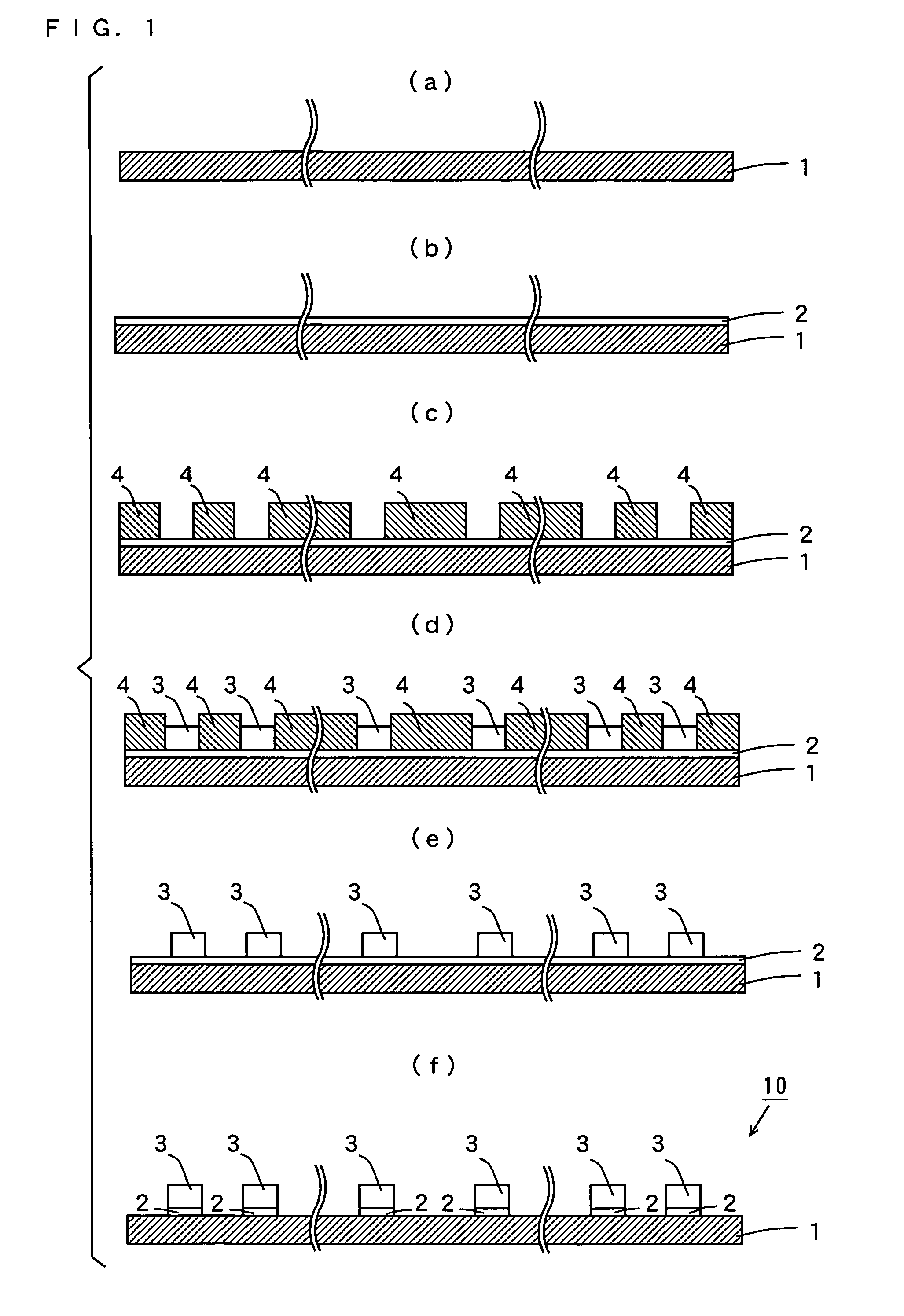
[0030]As the method of manufacturing the printed circuit board, a general semi-additive method is employed.

[0031]FIG. 1 is a schematic sectional view showing the steps in an example of the method of manufacturing a printed circuit board according to the semi-additive method.

[0032]As shown in FIG. 1(a), an insulating layer 1 of a polyimide film having a thickness of for example 25 μm is prepared.

[0033]Then, as shown in FIG. 1(b), a thin metal film 2 is formed by sputtering or electroless plating on the insulating layer 1. Note that the thin metal film 2 has a layered structure including a layer of nickel (Ni)-chromium (Cr) having a thickness of for example 40 nm and a layer of copper (Cu) having a thickness of for example 100 nm.

[0034]Now, as shown in FIG. 1(c), using dry film resist or the like, plating resist 4 in patterns reversed from conductive patterns (that will be described in connection with subsequent steps) is formed on the thin metal film 2.

[0035]Then, as shown in FIG. 1(...

second embodiment

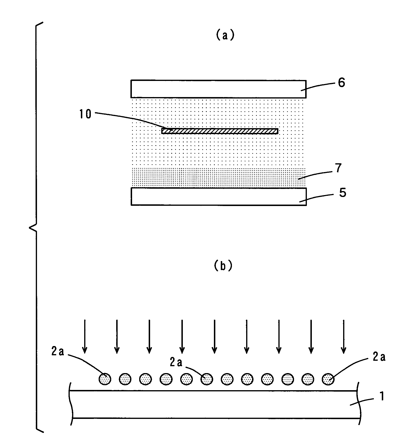
[0051]FIG. 3 is a schematic view of another example of how the printed circuit board 10 is processed by plasma etching.

[0052]As shown in FIG. 3, the printed circuit board 10 is provided for example on the earth electrode 6 provided in the plasma etching device. Note that if the AC electrode 5 contacts the printed circuit board 10, the printed circuit board 10 is damaged, and therefore the distance between the printed circuit board 10 and the AC electrode 5 is preferably not less than 1 mm.

[0053]The frequency of the AC power supply is preferably not more than 1 GHz. The pressure in the device is preferably atmospheric pressure (1.0×10⁵ Pa). The processing power is preferably from 500 W to 2000 W. The processing time is preferably from 10 seconds to 2 minutes.

[0054]The inter-electrode distance between the AC electrode 5 and the earth electrode 6 is preferably not more than 10 mm, more preferably from 1 mm to 5 mm. In this way, plasma discharge is carried out in a stable manner.

[0055]T...

third embodiment

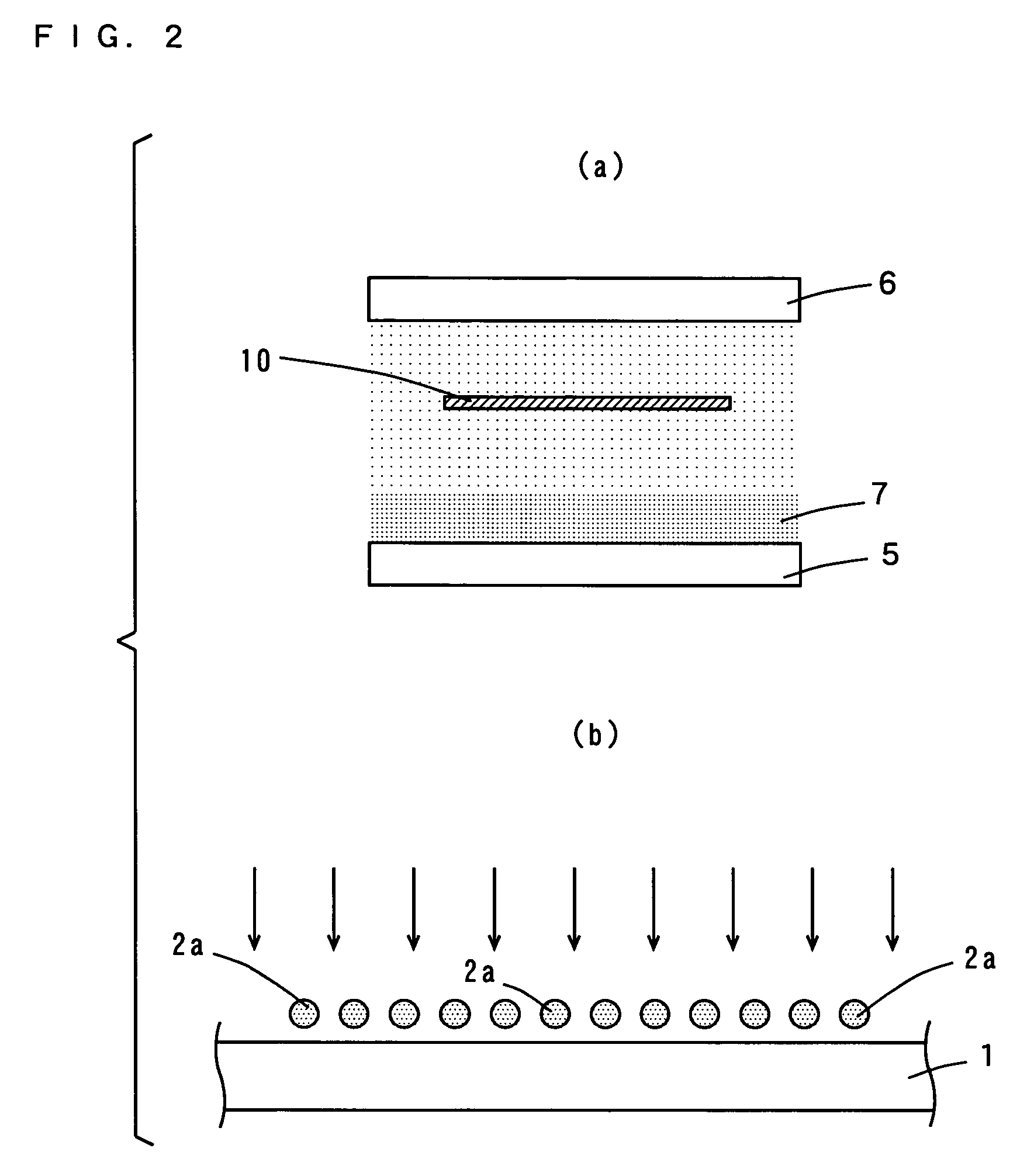
[0059]FIG. 4 is a schematic view of yet another example of how the printed circuit board 10 is processed by plasma etching.

[0060]As shown in FIG. 4, the printed circuit board 10 is provided for example in a chamber 8 in a magnetron type plasma etching device. Note that in FIG. 4, the printed circuit board 10 is placed about in the center of the chamber 8, but it may be placed in any position inside the chamber 8.

[0061]The frequency of the AC power supply is preferably not less than 1 GHz. The pressure in the chamber 8 is preferably from 1.33×10⁻² Pa to 1.33×10² Pa. The processing power is preferably from 400 W to 1000 W. The processing time is preferably from 20 seconds to 2 minutes.

[0062]The gas for the plasma etching is the same as that of the first embodiment.

[0063]According to the embodiment, plasma etching is carried out in the chamber 8 in the magnetron type plasma etching device, so that the sheath layer 7 does not form. In this way, isotropic etching is enabled.

[0064]As desc...


PUM

PropertyMeasurementUnit
thicknessaaaaaaaaaa
thicknessaaaaaaaaaa
pressureaaaaaaaaaa

Abstract

A printed circuit board having prescribed conductive patterns formed on an insulating layer is provided about 20 mm apart from an AC electrode provided in a plasma etching device. An earth electrode is provided on the side opposing the AC electrode. More specifically, the printed circuit board is provided outside a sheath layer that is a region having a high plasma density generated in the vicinity of the AC electrode. The frequency of an AC power supply is preferably not more than 1 GHz. The pressure in the device is preferably in the range from 1.33×10⁻² Pa to 1.33×10² Pa. The inter-electrode distance between the AC electrode and the earth electrode is preferably not more than 150 mm, more preferably from 40 mm to 100 mm.

Description

BACKGROUND OF THE INVENTION[0001]1. Field of the Invention[0002]The present invention relates to a method of manufacturing a printed circuit board.[0003]2. Description of the Background Art[0004]Printed circuit boards are generally produced by the semi-additive method. The semi-additive method includes the steps of forming a thin metal film on an insulating layer by sputtering, forming plating resist in a prescribed pattern on the thin metal film, forming conductive patterns in a region without the plating resist, removing the plating resist, and removing the exposed thin metal film by etching.[0005]In this case, after the exposed thin metal film is removed by etching according to the semi-additive method, a small amount of the residue of the metal film (hereinafter referred to as “residual metal”) may be left on the insulating layer.[0006]FIG. 5 shows schematic views of residual metal present on the insulating layer. As shown in FIG. 5(a), prescribed conductive patterns 3 are forme...

Claims


Application Information

Patent Timeline
Patent Type & Authority Patents(United States)
IPC IPC(8): H01B13/00
CPCC25D5/022H05K3/26H05K1/0346H05K3/108H05K2201/0761H05K2203/095
Inventor ODA, TAKASHI
Owner NITTO DENKO CORP
Why Eureka
Try Eureka