

Process For Thinning A Semiconductor Workpiece
a technology for workpieces and semiconductors, applied in semiconductor devices, semiconductor/solid-state device details, solid-state devices, etc., can solve the problems of icds operating at extremely high speeds, prone to heat generation, and conventional back grinding processes have drawbacks, so as to improve product structure, reduce the risk of breakage, and resist bowing and warping
- Summary
- Abstract
- Description
- Claims
- Application Information
AI Technical Summary
Benefits of technology
Problems solved by technology
Method used
Image

Examples
Embodiment Construction
Technical Field
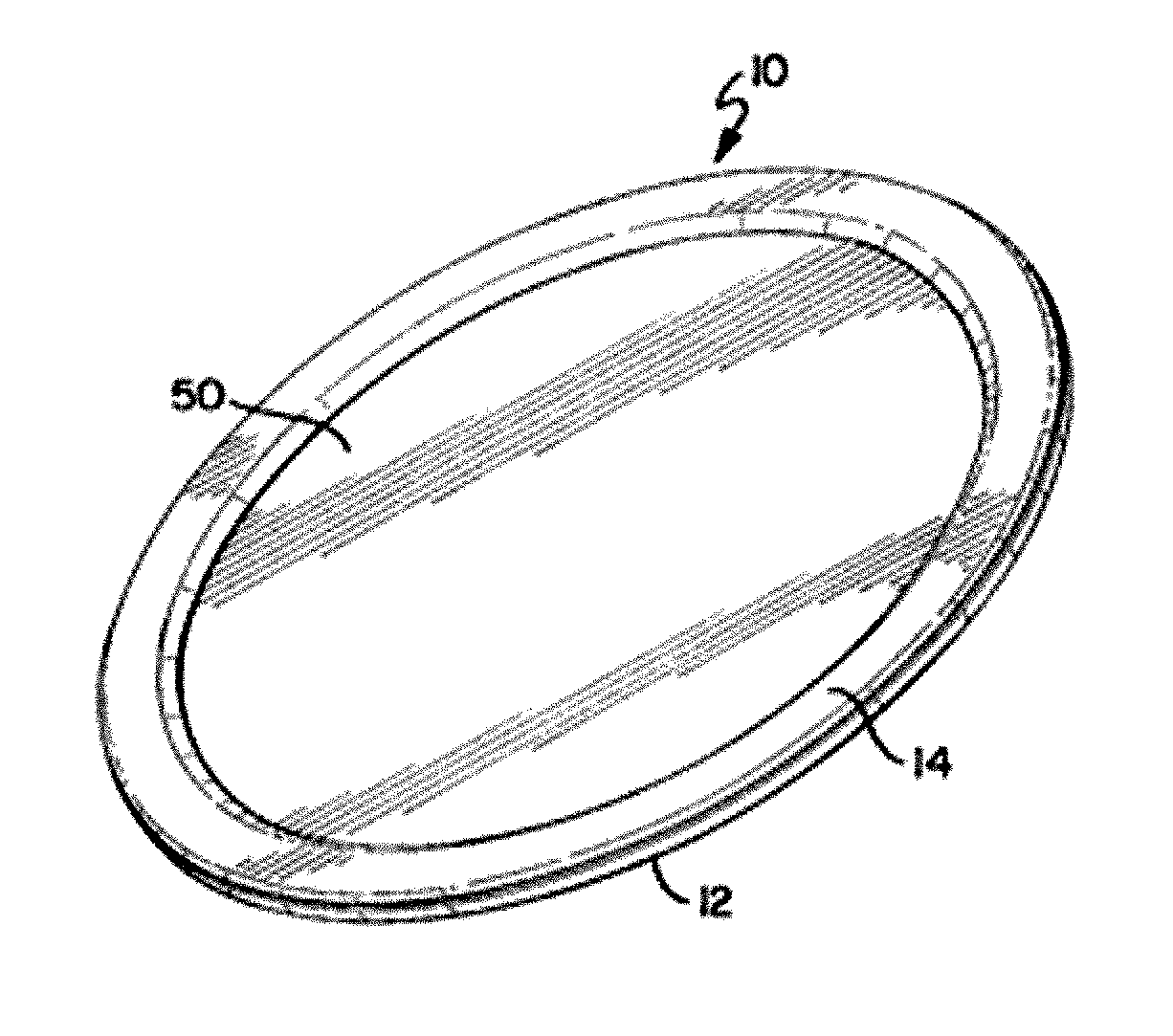
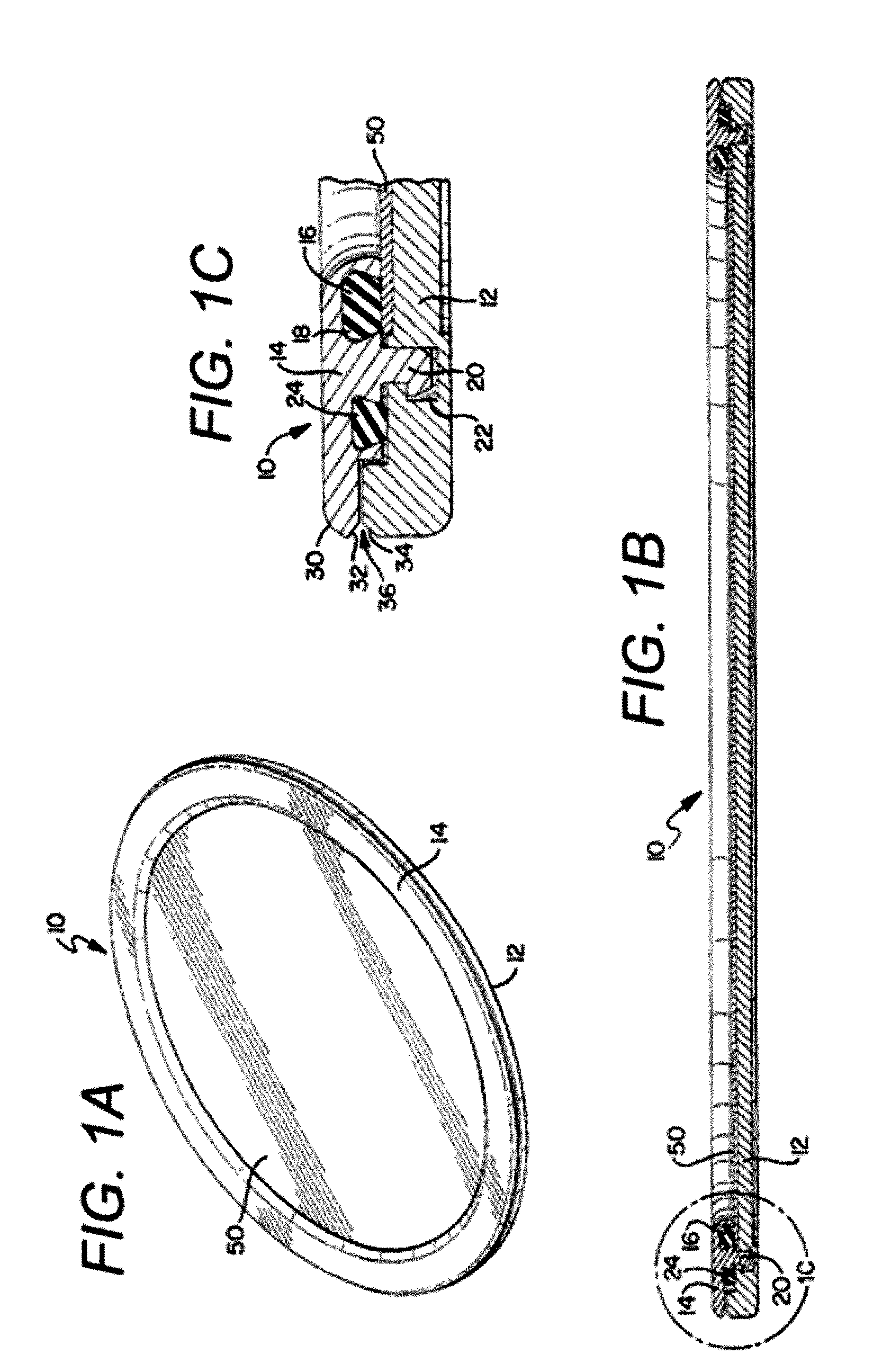
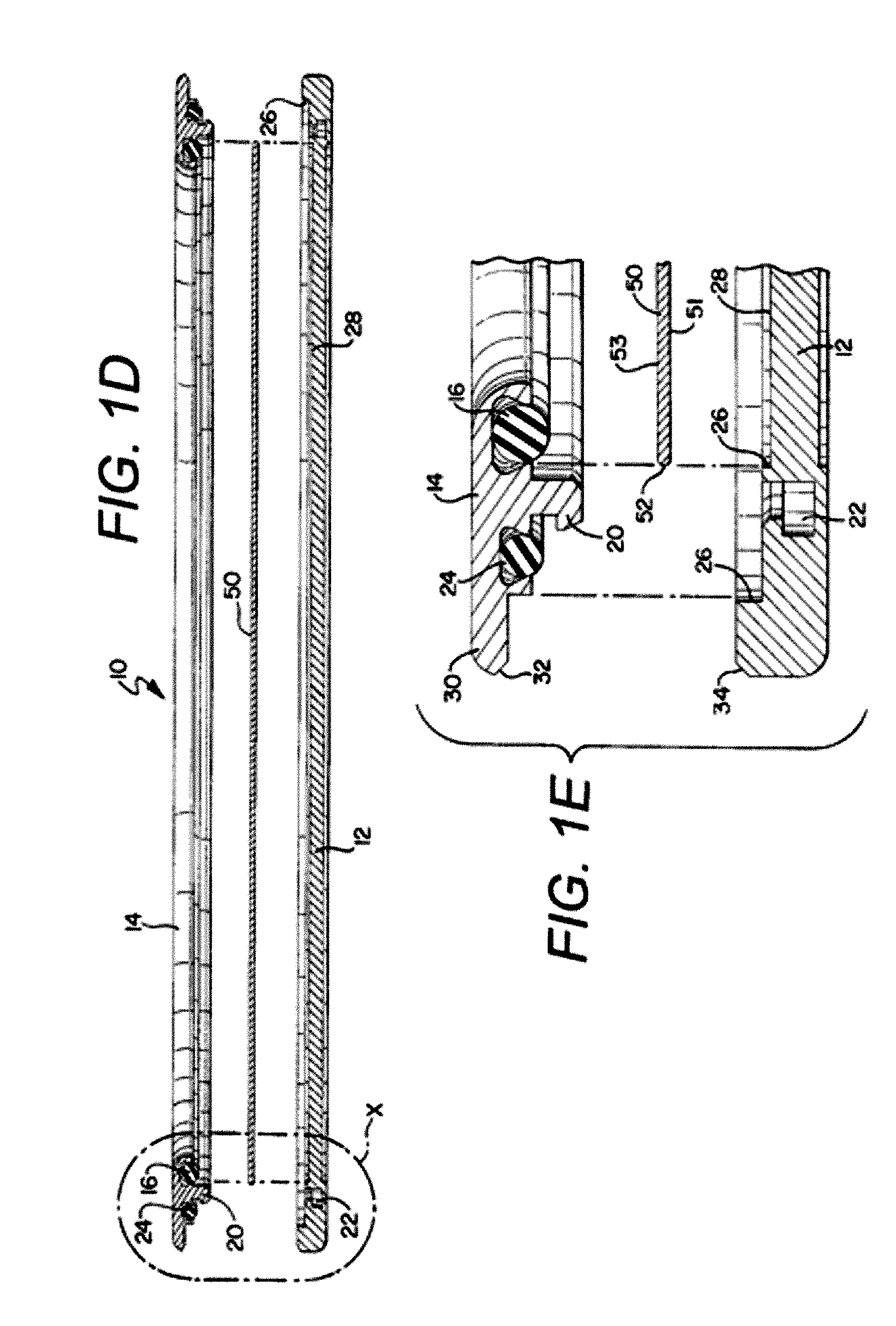
[0001] The invention relates to a process and apparatus for use with workpieces, such as semiconductor wafers, flat panel displays, rigid disk or optical media, thin film heads or other workpieces formed from a substrate on which microelectronic circuits, data storage elements or layers, or micro-mechanical elements may be formed. These and similar articles are collectively referred to herein as a “wafer” or “workpiece.” Specifically, the present invention relates to a process and apparatus for use in thinning semiconductor workpieces.
BACKGROUND OF THE INVENTION
[0002] State of the art electronics (e.g., cellular phones, personal digital assistants, and smart cards) demand thinner integrated circuit devices (“ICD”). In addition, advanced packaging of semiconductor devices (e.g., stacked dies or “flip-chips”) provide dimensional packaging constraints which also require an ultra-thin die. Moreover, as operating speeds of ICDs continue to increase heat dissipation becom...
PUM
| Property | Measurement | Unit |
|---|---|---|
| Length | aaaaa | aaaaa |
| Length | aaaaa | aaaaa |
| Length | aaaaa | aaaaa |
Abstract
Description
Claims
Application Information